. 2014 Dec 10;26(46):7747-63.
doi: 10.1002/adma.201304511. Epub 2014 Jun 23.

Coherent X-ray diffraction imaging and characterization of strain in silicon-on-insulator nanostructures

Affiliations
Free PMC article

Coherent X-ray diffraction imaging and characterization of strain in silicon-on-insulator nanostructures

Gang Xiong et al. Adv Mater. .
Free PMC article

Abstract

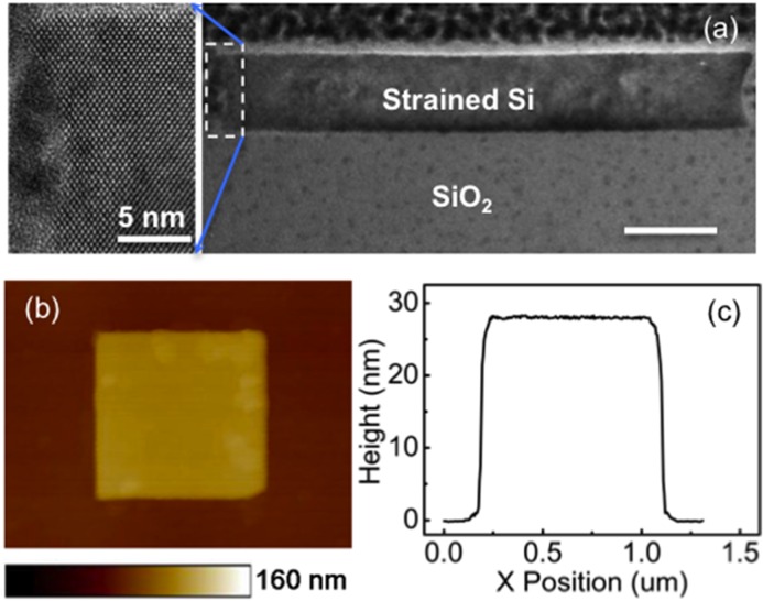
Coherent X-ray diffraction imaging (CDI) has emerged in the last decade as a promising high resolution lens-less imaging approach for the characterization of various samples. It has made significant technical progress through developments in source, algorithm and imaging methodologies thus enabling important scientific breakthroughs in a broad range of disciplines. In this report, we will introduce the principles of forward scattering CDI and Bragg geometry CDI (BCDI), with an emphasis on the latter. BCDI exploits the ultra-high sensitivity of the diffraction pattern to the distortions of crystalline lattice. Its ability of imaging strain on the nanometer scale in three dimensions is highly novel. We will present the latest progress on the application of BCDI in investigating the strain relaxation behavior in nanoscale patterned strained silicon-on-insulator (sSOI) materials, aiming to understand and engineer strain for the design and implementation of new generation semiconductor devices.

Keywords: coherent X-ray diffraction Imaging; nanowire; silicon-on-Insulator; strain; ultrathin layer.


Figures

Figure 1
Figure 1
Schematic views of (a) a lens-based imaging system and (b) a lens-less imaging system where the active area of the detector is highlighted with the blue colour. For lens-less imaging, the maximum spatial frequency collected in the diffraction pattern in principle determines the reconstruction resolution.
Figure 2
Figure 2
Sketch of three different imaging regions in lens-less imaging system defined as a function of the Fresnel distance formula image where a is the sample size and λ is the wavelength.
Figure 3
Figure 3
Process flow for a typical phase retrieval algorithm.
Figure 4
Figure 4
Experimental configuration for (a) plane-wave forward scattering CDI, in which a coherent beam illuminates the whole sample; and (b) Fresnel CDI in which a coherent phase-curved beam generated with Fresnel zone plate illuminates either a whole sample or part of a sample.
Figure 5
Figure 5
(a) Schematic view of a hexagonal-shaped crystal, where the dots correspond to lattice points (left); and the corresponding diffraction pattern in reciprocal space (right). Also shown here are the incoming (ki) and outgoing (kf) wave-vectors sketched according to the Ewald construction. As the crystal is rotated the diffraction patterns are collected by the detector (shown as a straight line perpendicular to the kf direction). (b) A crystal with the same size and shape as the one in (a), but with an edge dislocation inside the crystal (left); and the corresponding diffraction pattern in reciprocal space (right). (c) Typical experimental setup for Bragg CDI.
Figure 6
Figure 6
Biaxial tensile strain effects on the conduction and valence bands of silicon (100). (a) In the conduction band, the 6-fold degeneracy is lifted and electrons become repopulated into the lower energy Δ2 sub-band, which causes the average effective mass to decrease and inter-band scattering to reduce, therefore increasing the electron mobility; (b) in the valence band, The hole mobility enhancement is mainly due to the reduction of the phonon scattering caused by the lifting of the 2-fold degeneracy and lowering of the spin-off band.
Figure 7
Figure 7
Schematic presentation of the process flow for the fabrication of a sSOI wafer. (a) Growth of the relaxed SiGe substrate; (b) growth of the biaxially tensile strained Si on the SiGe substrate; (c) hydrogen ion implantation into the grown heterostructure; (d) bonding of the hydrogen implanted heterostructure to a SiO2/Si substrate; (e) thermal annealing induced layer exfoliation around the hydrogen implantation depth; (f) strained Si layer directly on SiO2/Si obtained after the removal of the residual SiGe with selective etch.
Figure 8
Figure 8
Schematic presentation of the process flow for patterning square strained silicon structures on a sSOI substrate, using E-beam lithography.
Figure 9
Figure 9
(a) High resolution TEM image of the edge profile of the strained-silicon-on-insulator structure after RIE etch; inset is the zoomed in view; (b) AFM image of a 20 nm thick 1 μm ×1 μm. strained Si structure and (c) the height profile across the center of the structure.
Figure 10
Figure 10
Schematic drawing of experimental geometry. The detector was positioned 1.5 m from the sample, with in-plane angle δ = 21.3°, out-of-plane angle γ = 14.6°, Bragg angle 2θ = 25.3° for Si (-111) diffraction.
Figure 11
Figure 11
(a) The 2D diffraction frame collected at the centre position of the rocking curve; (b) the 3D diffraction pattern obtained by stacking the collected 2D frames together, projected in the direction perpendicular to the sSOI thickness axis.
Figure 12
Figure 12
The reconstructed amplitude (a), phase (b), and a cross section plot of the phase variation along the x direction (black square), with the COMSOL-simulated displacement (red dashed line) (c).
Figure 13
Figure 13
Schematic side view of the modeling system (a) and the simulated in-plane displacement in the x direction (b). Reproduced with permission. 2011, American Institute of Physics.
Figure 14
Figure 14
Diffraction pattern (central frame of the (–111) reflection) for an array of 11 sSOI wires (a); and the reconstructed phase map with the amplitude (translucent white) superimposed (b). scale bar = 300 nm

Similar articles

Cited by

References

    1. Bartels RA, Paul A, Green H, Kapteyn HC, Murname MM, Backus S, Christov IP, Liu Yanwei, Attwood D, Jacobsen C. Science. 2002;297:376. - PubMed
    1. Takayama Y, Tai RZ, Hatano T, Miyhara T, Okamoto W, Kagoshima Y. J. Synchrotron Radiat. 1998;5:456. - PubMed
    1. van der Veen F, Pfeiffer F. J. Phys. Condens. Matter. 2004;16:5003.
    1. Vlieg E, de Vries SA, Alvarez J, Ferrer S. J. Synchrotron Radiat. 1997;4:210. - PubMed
    1. Bongaerts JHH, David C, Drakopoulos M, Zwanenburg MJ, Wegdam GH, Lackner T, Keymeulen H, vander Veen JF. J. Synchrotron Radiat. 2002;9:383.

LinkOut - more resources