. 2014 Jun 30:4:5486.
doi: 10.1038/srep05486.

Spin nano-oscillator-based wireless communication

Affiliations

Spin nano-oscillator-based wireless communication

Hyun Seok Choi et al. Sci Rep. .

Abstract

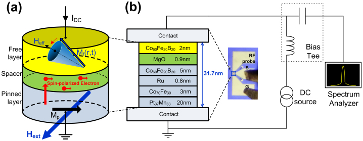
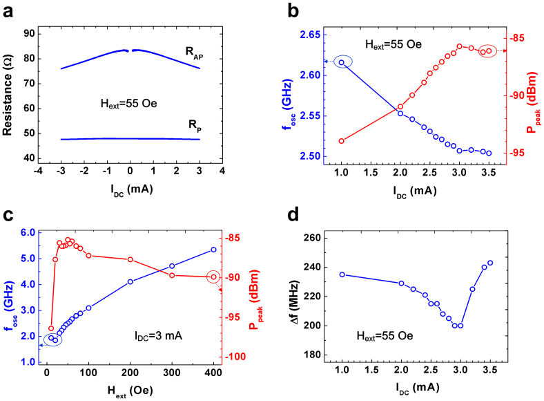
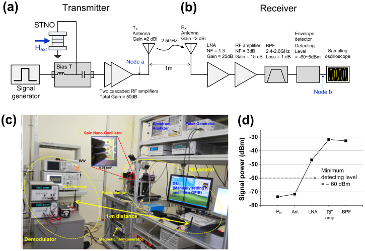
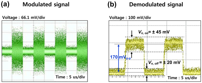
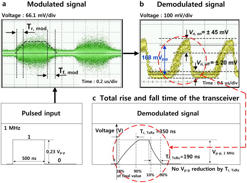
Spin-torque nano-oscillators (STNOs) have outstanding advantages of a high degree of compactness, high-frequency tunability, and good compatibility with the standard complementary metal-oxide-semiconductor process, which offer prospects for future wireless communication. There have as yet been no reports on wireless communication using STNOs, since the STNOs also have notable disadvantages such as lower output power and poorer spectral purity in comparison with those of LC voltage-controlled oscillators. Here we show that wireless communication is achieved by a proper choice of modulation scheme despite these drawbacks of STNOs. By adopting direct binary amplitude shift keying modulation and non-coherent demodulation, we demonstrate STNO-based wireless communication with 200-kbps data rate at a distance of 1 m between transmitter and receiver. It is shown, from the analysis of STNO noise, that the maximum data rate can be extended up to 1.48 Gbps with 1-ns turn-on time. For the fabricated STNO, the maximum data rate is 5 Mbps which is limited by the rise time measured in the total system. The result will provide a viable route to real microwave application of STNOs.


Figures

Figure 1
Figure 1. Operation and test setup of the STNO.
(a) Schematic of the STNO sample with a free layer (FL), a barrier, and a pinned layer (PL). Mp denotes the magnetization of the pinned layer, Mf(r,t) is the magnetization of the free layer, and Heff is the local effective magnetic field. (b) Schematic of the test setup for the STNO. Hext is the external magnetic field. Chip photo of the STNO (middle).
Figure 2
Figure 2. Characteristics of the measurements for the fabricated STNO.
(a) Magneto–resistance of the STNO as a function of IDC (Hext = 55 Oe). P indicates the parallel (P) state between Mp and Mf, AP denotes the antiparallel (AP) state between Mp and Mf. (b) The oscillation frequency fosc and peak output power Ppeak level of the STNO as a function of IDC (Hext = 55 Oe). (c) fosc and the Ppeak level of the STNO as a function of Hext (IDC = 3 mA). (d) The linewidth Δf of the STNO as a function of IDC (Hext = 55 Oe).
Figure 3
Figure 3. Configuration of the STNO–based binary ASK transceiver.
(a) Schematic of the STNO–based binary ASK transmitter (Tx). (b) Schematic of the receiver (Rx) and the gain and noise figure (NF) of the Rx chain. (c) The measurement set–up of the STNO–based binary ASK system. (d) The received signal power flow, where Pin is the received signal power of Rx and Ant, LNA, RF amp, and BPF are the measurement positions before the Rx antenna, the LNA, the RF amplifier, BPF, and the envelope detector, respectively. The signal level right after BPF is −32.7 dBm, which is within the detectable range of the demodulator (–60 ~ 5 dBm).
Figure 4
Figure 4. Modulated and demodulated signal in the time domain.
(a) The measured time trace of the modulated signal when the pulse frequency is 100 kHz at node a in Fig. 3a. (b) The measured time trace of the demodulated signal of 100 kHz at node b in Fig. 3b.
Figure 5
Figure 5. Rise and fall time of modulated and demodulated signal.
(a) The rise and fall time from the measured time trace of the modulated signal when the pulse frequency is 1 MHz at node a in Fig. 3a. (b) The measured time trace of the demodulated signal of 1 MHz at node b in Fig. 3b. (c) Total rise and fall time of the transceiver from the demodulated signal.

References

    1. Wolf S. A. et al. Spintronics: a spin-based electronics vision for future. Science 294, 1488–1495 (2001). - PubMed
    1. Villard P. U. et al. A GHz spintronic-based RF oscillator. IEEE J. Solid-State Circuits 45, 196–197 (2010).
    1. Krivorotov I. N. et al. Large-amplitude coherent spin waves excited by spin-polarized current in nanoscale spin valves. Phys. Rev. B 76, 024418 (2007).
    1. Ruotolo A. et al. Phase-locking of magnetic vortices mediated by antivortices. Nature Nanotechnology 4, 528–532 (2009). - PubMed
    1. KaKa S. et al. Mutual phase-locking of microwave spin torque nano-oscillators. Nature Letter 437, 389–392 (2005). - PubMed

Publication types