Review
. 2015 Jan 7;44(1):40-57.
doi: 10.1039/c4cs00131a. Epub 2014 Jun 30.

Optical characterization of single plasmonic nanoparticles

Affiliations
Review

Optical characterization of single plasmonic nanoparticles

Jana Olson et al. Chem Soc Rev. .

Abstract

This tutorial review surveys the optical properties of plasmonic nanoparticles studied by various single particle spectroscopy techniques. The surface plasmon resonance of metallic nanoparticles depends sensitively on the nanoparticle geometry and its environment, with even relatively minor deviations causing significant changes in the optical spectrum. Because for chemically prepared nanoparticles a distribution of their size and shape is inherent, ensemble spectra of such samples are inhomogeneously broadened, hiding the properties of the individual nanoparticles. The ability to measure one nanoparticle at a time using single particle spectroscopy can overcome this limitation. This review provides an overview of different steady-state single particle spectroscopy techniques that provide detailed insight into the spectral characteristics of plasmonic nanoparticles.


Figures
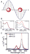
Fig. 1
Fig. 1
(A) Illustration of a localized surface plasmon for a spherical nanoparticle. (B) Mie theory calculation of the extinction (red), scattering (blue) and absorption (black) spectra of spherical gold nanoparticles with radii of 25 nm (left) and 50 nm (right). (C) Extinction (red), scattering (blue) and absorption (black) spectra calculated using Gans theory for ellipsoids with aspect ratio (AR) of 2.1 (solid line) and 3.0 (dotted symbol). The dielectric constant of the surrounding medium is chosen to be εm = 1 and 2.25 for calculations in (B) and (C), respectively.
Fig. 2
Fig. 2
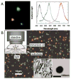
(A) Dark-field scattering image (left) of silver nanoparticles and their spectra (right), for which the colors of the curves are matched to the corresponding colors in the image. (B) True color scattering image of a sample consisting of gold nanorods (appearing as red dots) and 60 nm nanospheres (appearing as green dots) collected in dark-field illumination geometry as illustrated in the upper left inset. Bottom right insets: TEM images of nanorods and a nanosphere. Reprinted with permission from refs and . Copyright 2000 (ref 11) National Academy of Sciences, U.S.A., and Copyright 2002 (ref 13) American Physical Society.
Fig. 3
Fig. 3
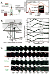
(A) Polarization sensitive dark-field scattering imaging of single gold nanorods, which appear as horizontally split doublets as indicated by pairs of red boxes. A birefringent crystal inserted before the CCD camera spatially separates orthogonal polarization components of the scattered light. Their relative intensities reflect the 2D orientations of the nanorods. (B) Top: Time trace of the total scattering intensity (black) and the respective intensities for the two orthogonal polarization components (red and green) recorded for a single nanorod. Bottom: Corresponding calculated 2D orientations of the nanorod as a function of time. Reprinted with permission from refs . Copyright 2005 American Chemical Society.
Fig. 4
Fig. 4
(A) Experimental realization of broadband extinction microscopy (left) and extinction spectrum of a single gold nanorod with a diameter of 120 nm (orange) and an aspect ratio of 3.1 (right). For comparison the scattering spectrum of a gold nanorod with a diameter of 24 nm (red) and the same aspect ratio is included. The inset shows SEM images of both nanorods. The sale bar is 100 nm. (B) Experimental scheme illustrating the interaction between a nanoparticle and the optical field in supercontinuum white light confocal microscopy (left) and normalized extinction spectra of single gold nanoparticles (right) with diameters of 60 (a), 31 (b), 20 (c), 10 (d) and 5 (e) nm. (C) Differential interference contrast microscopy images of two gold nanorods at 10 different orientations. The excitation wavelengths are 540 nm and 720 nm as indicated by the green and red frames for each image, respectively. Reprinted with permission from refs , and . Copyright 2010 (refs and 24) American Chemical Society, and Copyright 2004 (ref 22) American Physical Society.
Fig. 5
Fig. 5
(A) Experimental realization of spatial modulation spectroscopy. (B) Extinction spectra of a single silica shell coated silver nanoparticle (Ag@SiO2) excited with two orthogonal linear polarizations (red and blue symbols). The dashed lines are fits to a theoretical model assuming a spheroidal nanoparticle shape. Inset: Extinction spectrum of a single Ag@SiO2 nanoparticle compared to the ensemble spectrum of the colloidal solution. Reprinted with permission from ref . Copyright 2009 American Chemical Society.
Fig. 6
Fig. 6
(A) Experimental scheme of a photothermal imaging microscope (top) and 3D image (bottom left) and intensity histogram (bottom right) of 1.4 nm gold nanoparticles. (B) Top: SNR of the photothermal signal for 20 nm gold nanoparticle as a function of probe power. Middle: Relative SNR of the photothermal signal for 20 nm gold nanoparticles in different media plotted as a function of photothermal strength (see text for definition). Bottom: Histogram of the SNR of the photothermal signal for 20 nm gold nanoparticles deposited directly on glass (dark grey) and on a thermal isolation layer consisting of 100 nm thick polymer film on a glass substrate (light grey). The nanoparticles are covered with glycerol. Reprinted with permission from refs and . Copyright 2004 (ref 15) American Physical Society, and Copyright 2010 (ref 18) Royal Society of Chemistry.
Fig. 7
Fig. 7
(A) Correlated SEM (left) and photothermal (right) images of gold nanorods. (B) Photothermal intensity of two single gold nanorods and a dimer as a function of the polarization of the heating beam. The color of the traces correspond to the colored boxes in the SEM image. The orientation of the gold nanorods is determined from the polarization dependent photothernal intensity as is evident from the 90° phase shift of the green and red curves for the two perpendicularly orientated single nanorods. The wavelength of the heating beam at 675 nm is resonant with the longitudinal plasmon resonance of the nanorods. Reprinted with permission from ref . Copyright 2010 National Academy of Sciences, U.S.A.
Fig. 8
Fig. 8
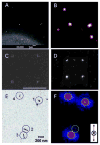
(A) SEM and (B) dark-field scattering images of single and clustered nanoshells. The bright region in (A) corresponds to a gold film that has been evaporated through a TEM finder grid with no carbon support film. (C) SEM and (D) dark-field scattering images of a correlation box etched into ITO coated glass by FIB milling. (E) TEM and (F) second harmonic optical images of nanoparticle dimers and nanorods. Correlation is achieved with the aid of electron beam lithography to prepare markers on a silicon nitride window, transparent in both a TEM and an optical microscope. Reprinted with permission from refs , , and . Copyright 2004 (ref 10) and 2005 (ref 37) American Chemical Society, and Copyright 2007 (ref 34) Wiley.
Fig. 9
Fig. 9
(A) TEM and (B) optical images of single Ag-Au hollow nanoparticles. (C) Scattering spectra of a hollow nanoparticle taken before (green) and after (red) TEM imaging. (D) Histogram of resonance energies of hollow nanoparticles before (green) and after (red) exposure to an electron beam. Reprinted with permission from ref . Copyright 2008 American Chemical Society.
Fig. 10
Fig. 10
(A–H) Super-resolution fluorescence imaging of a plasmonic nanowire using GSDIM. (A) Scattering and (B) far-field fluorescence images with of a gold nanowire. Super-resolution images constructed from the frequency histogram (C) and spatial intensity map (D) of individual fluorescence events. (E) SEM image of the nanowire and (F) enhanced SEM image to show the contrast of the nanowire edges. (G) Intensity histogram overlaid with the SEM image from (F). (H) Intensity histogram overlaid with the fluorescence image from (B). The scale bar in all images is 500 nm. (I–N) Super-resolution fluorescence imaging of plasmonic nanotriangles using PALM. (I) AFM image of a gold nanotriangle array. Super-resolution images constructed from the frequency histogram (J) and spatial intensity map (K) of the gold nanotriangles highlighted by the larger white box in (I). (L–N) Examples of high-resolution density maps of the individual gold nanotriangles marked by the dashed squares in (I). Reprinted with permission from refs and . Copyright 2013 (ref 40) Royal Society of Chemistry, and Copyright 2012 (ref 41) Wiley.
Fig. 11
Fig. 11
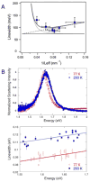
(A) Plasmon linewidth as function of 1/Leff for gold nanorods with aspect ratios between 2 and 4. Lines are the calculated linewidth from bulk damping (horizontal line), bulk damping plus electron surface scattering (dashed line), and bulk damping plus radiation damping (dotted line). The solid line shows the total linewidth resulting from all three contributions. (B) Single particle scattering spectra of gold bipyramids at 293 K and 77 K (top) and plasmon linewidth as a function of resonance energy for single bipyramids measured at these two temperatures (bottom). Reprinted with permission from refs and . Copyright 2006 (ref 8) Royal Society of Chemistry, and Copyright 2009 (ref 45) American Physical Society.
Fig. 12
Fig. 12
(A) Plasmon linewidths as a function of resonance energy for single gold nanorod on quartz (ΓQ, blue stars) and data binned in 0.03 eV intervals (ΓQ bin, blue circles) are compared to the linewidths calculated using a quasi-static model (ΓQSM, gray line) and FDTD simulations (ΓFDTD, purple circles). (B) Plasmon linewidths for single gold nanorods on graphene (ΓG, orange stars) and data binned in 0.03 eV intervals (ΓG bin, orange circles) are compared to the binned values measured for nanorods on quartz (ΓQ bin, blue circles) and the quasi-static model (ΓQSM, gray line). (C) Schematic energy diagram illustrating charge transfer between a gold nanorod (left) and graphene (right) following plasmon induced hot electron generation. Reprinted with permission from ref . Copyright 2013 American Chemical Society.

References

    1. Kreibig U, Vollmer M. Optical properties of metal clusters. Springer; Berlin: 1995.
    1. Bohren CF, Huffman DR. Absorption and Scattering of Light by Small Particles. WILEY-VCH Verlag GmbH & Co. KGaA; Weinheim: 1983.
    1. Lal S, Grady NK, Kundu J, Levin CS, Lassiter JB, Halas NJ. Chem Soc Rev. 2008;37:898–911. - PubMed
    1. Hu M, Chen J, Li ZY, Au L, Hartland GV, Li X, Marquez M, Xia Y. Chem Soc Rev. 2006;35:1084–1094. - PubMed
    1. Willets KA, Van Duyne RP. Annual Review of Physical Chemistry. 2007;58:267–297. - PubMed

Publication types