

Heterogeneous integration of epitaxial Ge on Si using AlAs/GaAs buffer architecture: suitability for low-power fin field-effect transistors
- PMID: 25376723
- PMCID: PMC4223664
- DOI: 10.1038/srep06964
Heterogeneous integration of epitaxial Ge on Si using AlAs/GaAs buffer architecture: suitability for low-power fin field-effect transistors
Abstract
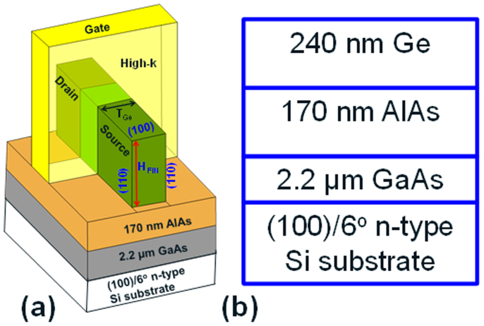
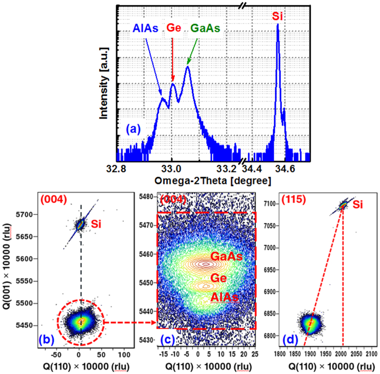
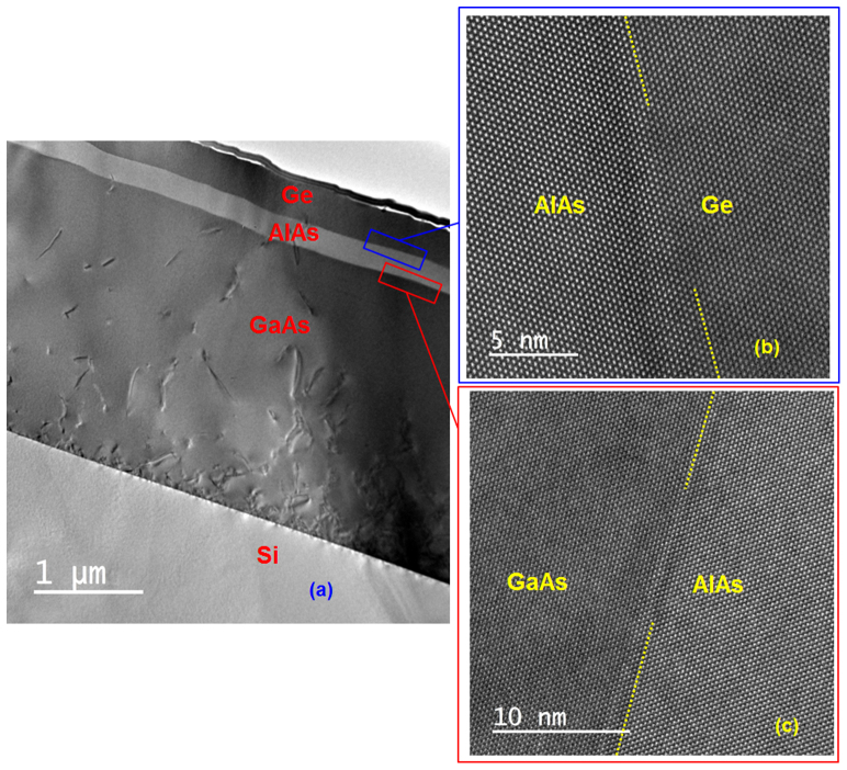
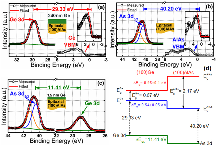
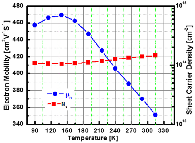
Germanium-based materials and device architectures have recently appeared as exciting material systems for future low-power nanoscale transistors and photonic devices. Heterogeneous integration of germanium (Ge)-based materials on silicon (Si) using large bandgap buffer architectures could enable the monolithic integration of electronics and photonics. In this paper, we report on the heterogeneous integration of device-quality epitaxial Ge on Si using composite AlAs/GaAs large bandgap buffer, grown by molecular beam epitaxy that is suitable for fabricating low-power fin field-effect transistors required for continuing transistor miniaturization. The superior structural quality of the integrated Ge on Si using AlAs/GaAs was demonstrated using high-resolution x-ray diffraction analysis. High-resolution transmission electron microscopy confirmed relaxed Ge with high crystalline quality and a sharp Ge/AlAs heterointerface. X-ray photoelectron spectroscopy demonstrated a large valence band offset at the Ge/AlAs interface, as compared to Ge/GaAs heterostructure, which is a prerequisite for superior carrier confinement. The temperature-dependent electrical transport properties of the n-type Ge layer demonstrated a Hall mobility of 370 cm(2)/Vs at 290 K and 457 cm(2)/Vs at 90 K, which suggests epitaxial Ge grown on Si using an AlAs/GaAs buffer architecture would be a promising candidate for next-generation high-performance and energy-efficient fin field-effect transistor applications.
Figures
References
-
- Moore G. No Exponential is Forever: But “Forever” Can Be Delayed!. Solid-State Circuits Conference, 2003. Digest of Technical Papers. ISSCC. 2003 IEEE International 10-13 Feb. 2003, San Francisco, CA, IEEE, pp. 20–23 (2003) (10.1109/ISSCC.2003.1234194).
-
- International Technology Roadmap for Semiconductors. (2013); http://www.itrs.net/Links/2013ITRS/2013Chapters/2013PIDS_Summary.pdf (05/10/2014).
-
- Kavalieros J. T. et al. Tri-Gate Transistor Architecture with High-k Gate Dielectrics, Metal Gates and Strain Engineering. International Symposium on VLSI Technology, Systems, and Applications pp. 50–51 (2006). Honolulu, HI; IEEE (10.1109/VLSIT.2006.1705211); June 13th, 2006.
-
- Heyns M. et al. Advancing CMOS beyond the Si roadmap with Ge and III/V devices. Electron Devices Meeting (IEDM), 2011 IEEE International, 5–7 Dec. 2011, Washington, DC, IEEE, pp. 13.1.1–13.1.4 (2011) (10.1109/IEDM.2011.6131543).
-
- Mitard J. et al. Record ION/IOFF performance for 65 nm Ge pMOSFET and novel Si passivation scheme for improved EOT scalability. Electron Devices Meeting (IEDM), 2008 IEEE International 15–17 Dec. 2008, San Francisco, CA, IEEE, pp. 873–876 (2008) (10.1109/IEDM.2008.4796837).
Publication types
LinkOut - more resources
Full Text Sources
Other Literature Sources
