. 2014 Dec 10:5:5714.
doi: 10.1038/ncomms6714.

Laser-induced porous graphene films from commercial polymers

Affiliations

Laser-induced porous graphene films from commercial polymers

Jian Lin et al. Nat Commun. .

Abstract

The cost effective synthesis and patterning of carbon nanomaterials is a challenge in electronic and energy storage devices. Here we report a one-step, scalable approach for producing and patterning porous graphene films with three-dimensional networks from commercial polymer films using a CO2 infrared laser. The sp3-carbon atoms are photothermally converted to sp2-carbon atoms by pulsed laser irradiation. The resulting laser-induced graphene (LIG) exhibits high electrical conductivity. The LIG can be readily patterned to interdigitated electrodes for in-plane microsupercapacitors with specific capacitances of >4 mF cm-2 and power densities of ~9 mW cm-2. Theoretical calculations partially suggest that enhanced capacitance may result from LIG's unusual ultra-polycrystalline lattice of pentagon-heptagon structures. Combined with the advantage of one-step processing of LIG in air from commercial polymer sheets, which would allow the employment of a roll-to-roll manufacturing process, this technique provides a rapid route to polymer-written electronic and energy storage devices.


Figures
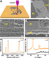
Figure 1
Figure 1. LIG formed from commercial PI films using a CO2 laser at a power of 3.6 W to write patterns
a, Schematic of the synthesis process of LIG from PI. b, SEM image of LIG patterned into an owl shape; scale bar, 1 mm. The bright contrast corresponds to LIG surrounded by the darker-colored insulating PI substrates. c, SEM image of the LIG film circled in b; scale bar, 10 µm. Inset is the corresponding higher magnification SEM image; scale bar, 1 µm. d, Cross-sectional SEM image of the LIG film on the PI substrate; scale bar, 20 µm. Inset is the SEM image showing the porous morphology of LIG; scale bar, 1 µm. e, Representative Raman spectrum of a LIG film and the starting PI film. f, XRD of powdered LIG scraped from the PI film.
Figure 2
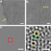
Figure 2. TEM images of LIG obtained with a laser power of 3.6 W
a, HRTEM image taken at the edge of a LIG flake showing few-layer features and highly wrinkled structures; scale bar, 10 nm. b, HRTEM image of LIG; scale bar, 5 nm. Average lattice space of ~3.4 Å corresponds to the (002) planes of graphitic materials. c, Cs-correction STEM image taken at the edge of a LIG flake; scale bar, 2 nm. It shows an ultra-polycrystalline nature with grain boundaries. d, TEM image of selected area indicated as a rectangle in c. It shows a heptagon with two pentagons as well as a hexagon; scale bar, 5 Å.
Figure 3
Figure 3. Characterizations of LIG prepared with different laser powers
a, Atomic percentages of carbon, oxygen and nitrogen as a function of laser power. These values are obtained from high-resolution XPS. The threshold power is 2.4 W, at which conversion from PI to LIG occurs. b, Correlations of the sheet resistance and LIG film thicknesses with laser powers. c, Raman spectra of LIG films obtained with different laser powers. d, Statistical analysis of ratios of G and D peak intensities (upper panel), and average domain size along a-axis (La) as a function of laser power (x axis) calculated using eq 4.
Figure 4
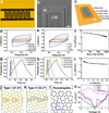
Figure 4. Electrochemical performances of LIG-MSC devices from LIG-4.8 W in 1 M H2SO4 with their GB-induced properties
a, A digital photograph of LIG-MSCs with 12 interdigital electrodes; scale bar, 1 mm. b, SEM image of LIG electrodes; scale bar, 200 µm. c, Schematic diagram of LIG-MSCs device architecture. d and e, CV curves of LIG-MSCs at scan rates from 20 to 10,000 mV·s−1. f, Specific areal capacitance (CA) calculated from CV curves as a function of scan rates. g and h, CC curves of LIG-MSCs at discharge current densities (ID) varied from 0.2 to 25 mA·cm−2. I, CA calculated from CC curves vs. ID. j and k, Charge density distribution of the states within a voltage window (−0.1, 0.1) V for type I and II polycrystalline sheets. The defects at the grain boundaries are shadowed, and numbers show the misorientation angle between the grains. l, A carbon layer fully composed of pentagons and heptagons (pentaheptite). n, Calculated quantum capacitance (defined in the text) of perfect and polycrystalline/disordered graphene layers.

References

    1. Geim AK. Graphene: status and prospects. Science. 2009;324:1530–1534. - PubMed
    1. Chen ZP, et al. Three-dimensional flexible and conductive interconnected graphene networks grown by chemical vapour deposition. Nat. Mater. 2011;10:424–428. - PubMed
    1. Wang XB, et al. Three-dimensional strutted graphene grown by substrate-free sugar blowing for high-power-density supercapacitors. Nat. Commun. 2013;4 - PMC - PubMed
    1. Miller JR, Outlaw RA, Holloway BC. Graphene double-layer capacitor with ac line-filtering performance. Science. 2010;329:1637–1639. - PubMed
    1. Wu ZS, et al. Three-dimensional nitrogen and boron co-doped graphene for high-performance all-solid-state supercapacitors. Adv. Mater. 2012;24:5130–5135. - PubMed