Review
. 2015 Jul-Aug;7(4):475-93.
doi: 10.1002/wnan.1323. Epub 2014 Dec 22.

Single-molecule bioelectronics

Affiliations
Review

Single-molecule bioelectronics

Jacob K Rosenstein et al. Wiley Interdiscip Rev Nanomed Nanobiotechnol. 2015 Jul-Aug.

Abstract

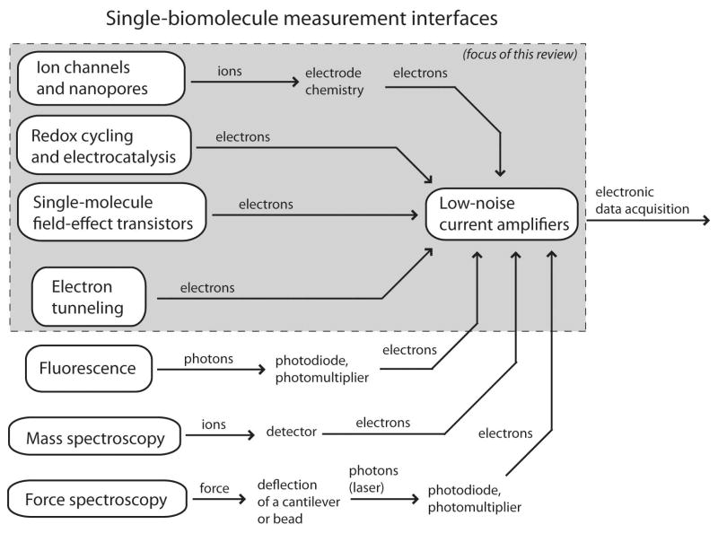
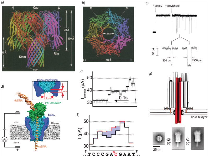
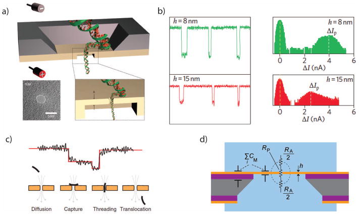
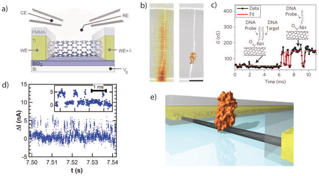
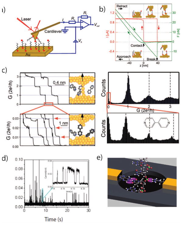
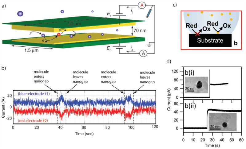
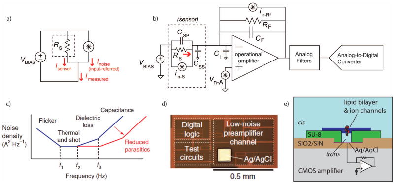
Experimental techniques that interface single biomolecules directly with microelectronic systems are increasingly being used in a wide range of powerful applications, from fundamental studies of biomolecules to ultra-sensitive assays. In this study, we review several technologies that can perform electronic measurements of single molecules in solution: ion channels, nanopore sensors, carbon nanotube field-effect transistors, electron tunneling gaps, and redox cycling. We discuss the shared features among these techniques that enable them to resolve individual molecules, and discuss their limitations. Recordings from each of these methods all rely on similar electronic instrumentation, and we discuss the relevant circuit implementations and potential for scaling these single-molecule bioelectronic interfaces to high-throughput arrayed sensing platforms.


Figures

Figure 1
Figure 1
An overview of available classes of single-molecule measurements. The signal path of all of these systems begins with conversion of a molecular state into a stream of ions, photons, electrons, or force, and the strength of this initial transduction often determines the overall signal quality. Eventually, the transduced signal is converted into an electronic current, which is them amplified and connected with other electronic systems. This review focuses on the highlighted platforms, which are physically small and entirely electrochemical.
Figure 2
Figure 2
a. Protein structure of alpha hemolysin (α-HL), a bacterial toxin which self-assembles through cell membranes. b. Top view of the α-HL structure, showing its open center which allows ions to pass through cell membranes and can be used as a nanopore sensor. c. Electric fields can induce single-stranded DNA molecules to pass through the α-HL pore, transiently reducing the ionic conductance. d. Enzymes such as DNA polymerase can be paired with nanopores to control the translocation velocity. e. Polymerase rachets a DNA molecule through a nanopore one base at a time, leaving behind a stepwise residual current. f. The residual current is sensitive to the DNA base composition, such as the methylated-C substitution shown here. g. Other biomolecular structures can also be used to construct nanopores, such as DNA origami. Images a+b are from , with permission. Image c is from , with permission. Images d–f are from , with permission. Image g is from , with permission.
Figure 3
Figure 3
a. An illustration of a double-stranded DNA molecule passing through a solid-state nanopore. Inset, a TEM image of a silicon nitride nanopore. b. Current signals from translocations through SiNx nanopores can be as large as several nanoamperes. c. Nanopore current blockades are sensitive to the orientation and position of a translocating molecule. d. Simplified electrical equivalent circuit of a solid-state nanopore, highlighting the access resistance RA and the membrane capacitance CM. Images a+b are from , with permission. Images c+d are from , with permission.
Figure 4
Figure 4
a. An illustration of a liquid-gated field-effect transistor made from a single carbon nanotube. b. Scanning gate microscopy images of a CNT-FET before and after point functionalization. The CNT is chemically modified so that its conductance is predominantly controlled by the electrostatics at a single defect site. c. A time trace from a carbon nanotube modified with a DNA probe molecule. The CNT exhibits two discrete conductance levels, corresponding to the hybridization and melting of a complementary DNA molecule. d. An SMFET trace with an attached enzyme, showing discrete conductance levels that correspond to the states within the activity of the enzyme. e. A rendering of an enzyme tethered to an SMFET. Image a is from , with permission. Images b+c are from , with permission. Images d+e are from , with permission.
Figure 5
Figure 5
a. A schematic of a typical scanning probe microscopy (SPM) experiment for single-molecule conductance measurements. A conductive cantilever is brought in contact with a conductive surface, under an electrical bias voltage (Vb), while the current (I) through the probe is monitored. The deflection of the cantilever can be monitored using a reflected laser to infer the applied mechanical force. b. The probe is brought repeatedly into contact with the surface and withdrawn. As the probe withdraws, it forms a transient single-atom wire junction. c. Monitoring the current through the probe during its withdrawal displays quantized conductance, and after the metal junction breaks, analyte molecules can enter the junction. Histograms from many wire-pull experiments can highlight the conductances of single analyte molecules. d. If the SPM tip is held at a constant distance from the surface, analyte molecules can diffuse into the junction, creating transient spike trains. e. A rendering of a proposed DNA sequencing platform utilizing nanoelectrodes functionalized with recognition molecules that record tunneling currents through a DNA molecule as it passes through a nanopore. Image a+b are from , with permission Image c is from , with permission Image d is from , with permission Image e is from , with permission
Figure 6
Figure 6
a. An illustration of a redox cycling measurement, in which a single analyte molecule diffuses between two closely spaced electrodes and is alternatively oxidized and reduced. b. Representative single-molecule data from a redox-cycling experiment. As molecules diffuse in and out of the region between the two electrodes, the measured current changes. c. An illustration of electrocatalysis, in which surface-bound catalysts enable electrochemical reactions at rates far exceeding those with a bare electrode surface. d. Current traces from the arrival of single nanoparticle catalysts at an electrode surface. Images a is from , with permission. Image b is adapted from , with permission. Images c+d are from , with permission.
Figure 7
Figure 7
a. Electronic nanosensors are often arranged in a configuration which measures their current (ISENSOR) while applying a constant voltage (VBIAS) across the device. Variance in the measurement can be represented by an input-referred equivalent noise source, whose current (INOISE) is added to the desired value. b. A simplified schematic of a low-noise current preamplifier connected to a device modeled as a resistor, RS, with parasitic capacitances (CSP and CSS). The operational amplifier has its own input capacitance (CI) and feedback capacitance (CF). Noise sources are also noted in the figure including the input-referred voltage noise of the amplifier (vn-A), the thermal noise of the feedback resistor (in-Rf), and the noise of the sensor itself (in-S). c. Representative current noise power spectral density at the input of the current preamplifier. Below the frequency f1, the noise is dominated by the flicker noise of the transducer. Between f1 and f2, the thermal noise of the transducer and the feedback resistor of the preamplifier set the noise floor. Flicker noise in the amplifier or imperfect dielectrics in the transducer provide a ∝f slope between f2 and f3. Above f3, the input-referred noise acquires a ∝f2 slope due to the noise of the amplifier acting through ΣCIN. This noise can be greatly reduced by scaling down the physical dimensions of the sensors, fluidics, interconnects, and electronic circuits. d. A micrograph of a low-noise current preamplifier implemented in a modern CMOS process. e. An illustration of a lipid bilayer reconstituted on the surface of an integrated circuit amplifier chip, reducing interconnects and relevant capacitances. Images c+d are from , with permission. Image e is from , with permission.

References

    1. Eid J, Fehr A, Gray J, Luong K, Lyle J, Otto G, Peluso P, Rank D, Baybayan P, Bettman B, et al. Science. 2009;323:133. - PubMed
    1. Eisenstein M. Nature biotechnology. 2012;30:295. - PubMed
    1. Fenn J, Mann M, Meng C. Science. 1989
    1. Hansma H, Hoh J. Annual review of biophysics and biomolecular structure. 1994 - PubMed
    1. Hille B. 2001

Publication types