

Fabrication of two dimensional polyethylene terephthalate nanofluidic chip using hot embossing and thermal bonding technique
- PMID: 25553203
- PMCID: PMC4247375
- DOI: 10.1063/1.4902945
Fabrication of two dimensional polyethylene terephthalate nanofluidic chip using hot embossing and thermal bonding technique
Abstract
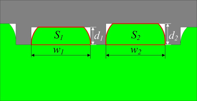
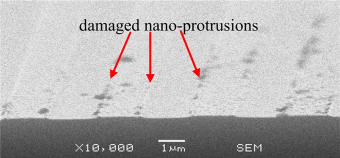
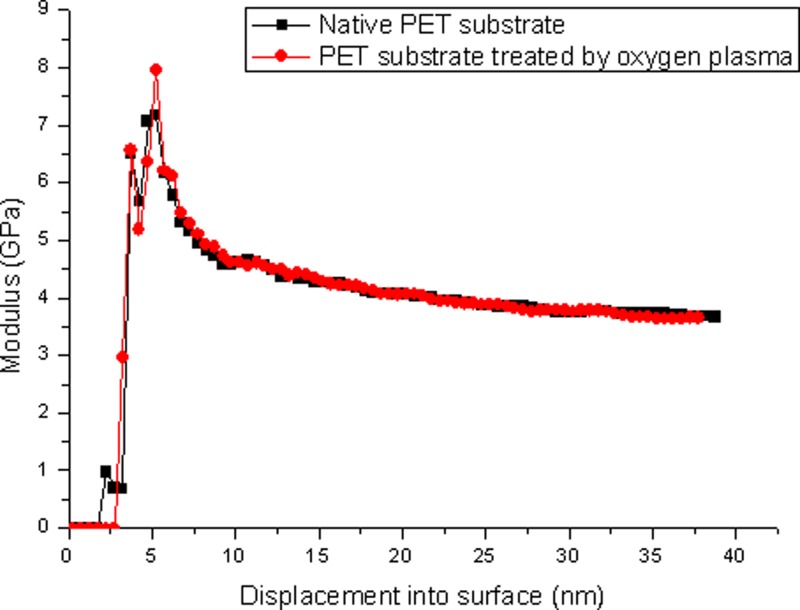
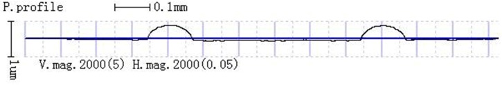
We present in this paper a method for obtaining a low cost and high replication precision 2D (two dimensional) nanofluidic chip with a PET (polyethylene terephthalate) sheet, which uses hot embossing and a thermal bonding technique. The hot embossing process parameters were optimized by both experiments and the finite element method to improve the replication precision of the 2D nanochannels. With the optimized process parameters, 174.67 ± 4.51 nm wide and 179.00 ± 4.00 nm deep nanochannels were successfully replicated into the PET sheet with high replication precision of 98.4%. O2 plasma treatment was carried out before the bonding process to decrease the dimension loss and improve the bonding strength of the 2D nanofluidic chip. The bonding parameters were optimized by bonding rate of the nanofluidic chip. The experiment results show that the bonding strength of the 2D PET nanofluidic chip is 0.664 MPa, and the total dimension loss of 2D nanochannels is 4.34 ± 7.03 nm and 18.33 ± 9.52 nm, in width and depth, respectively. The fluorescence images demonstrate that there is no blocking or leakage over the entire micro- and nanochannels. With this fabrication technology, low cost polymer nanochannels can be fabricated, which allows for commercial manufacturing of nano-components.
Figures


Similar articles
-
Two dimensional PMMA nanofluidic device fabricated by hot embossing and oxygen plasma assisted thermal bonding methods.Nanotechnology. 2015 May 29;26(21):215302. doi: 10.1088/0957-4484/26/21/215302. Epub 2015 May 7. Nanotechnology. 2015. PMID: 25946991
-
Polycarbonate Nanofluidic Chip Fabrication Technique by Hot Embossing and Thermal Bonding.J Nanosci Nanotechnol. 2018 Apr 1;18(4):2530-2535. doi: 10.1166/jnn.2018.14341. J Nanosci Nanotechnol. 2018. PMID: 29442923
-
A novel hybrid patterning technique for micro and nanochannel fabrication by integrating hot embossing and inverse UV photolithography.Lab Chip. 2014 May 7;14(9):1614-21. doi: 10.1039/c3lc51369f. Epub 2014 Mar 20. Lab Chip. 2014. PMID: 24647653
-
Fabrication of SU-8 polymer micro/nanoscale nozzle by hot embossing method.Nanotechnology. 2024 Apr 4;35(25). doi: 10.1088/1361-6528/ad3252. Nanotechnology. 2024. PMID: 38467057
-
Fabrication of nanofluidic biochips with nanochannels for applications in DNA analysis.Small. 2012 Sep 24;8(18):2787-801. doi: 10.1002/smll.201200240. Epub 2012 Jul 9. Small. 2012. PMID: 22778064 Review.
Cited by
-
Low auto-fluorescence fabrication methods for plastic nanoslits.IET Nanobiotechnol. 2016 Apr;10(2):75-80. doi: 10.1049/iet-nbt.2015.0045. IET Nanobiotechnol. 2016. PMID: 27074857 Free PMC article.
References
-
- Eijkel J. C. T. and Berg A. van den, Microfluid. Nanofluid. 1, 249 (2005).10.1007/s10404-004-0012-9 - DOI
-
- Anwar K., Han T., and Kim S. M., in Fluid Measurements and Instrumentation Cavitation and Multiphase Flow Advances in Fluids Engineering Education Microfluidics (2012), Vol. 2, p. 409.
LinkOut - more resources
Full Text Sources
Other Literature Sources