Review
. 2015 Feb 21;15(4):971-990.
doi: 10.1039/c4lc01208a.

Two-dimensional photonic crystals for sensitive microscale chemical and biochemical sensing

Affiliations
Review

Two-dimensional photonic crystals for sensitive microscale chemical and biochemical sensing

James E Baker et al. Lab Chip. .

Abstract

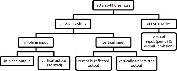
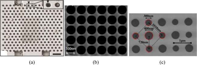
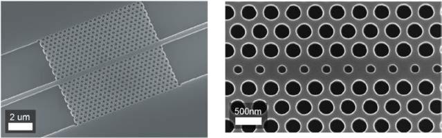
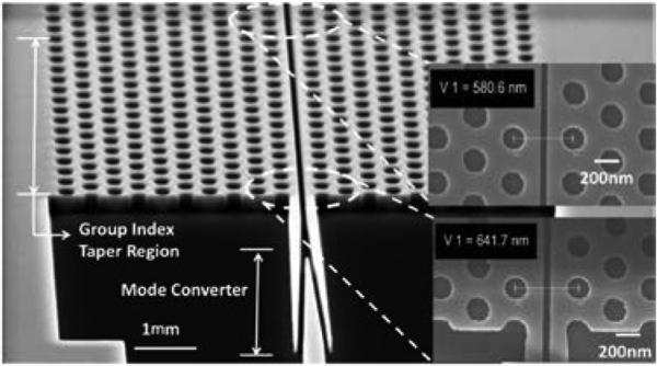
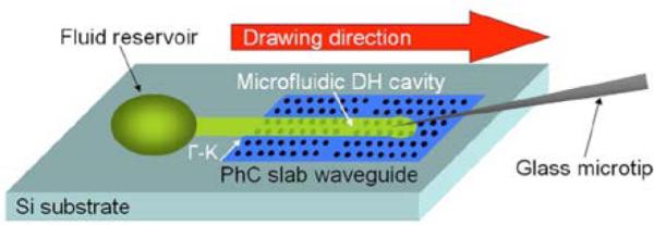
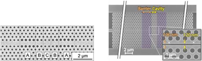
Photonic crystals - optical devices able to respond to changes in the refractive index of a small volume of space - are an emerging class of label-free chemical- and bio-sensors. This review focuses on one class of photonic crystal, in which light is confined to a patterned planar material layer of sub-wavelength thickness. These devices are small (on the order of tens to hundreds of microns square), suitable for incorporation into lab-on-a-chip systems, and in theory can provide exceptional sensitivity. We introduce the defining characteristics and basic operation of two-dimensional photonic crystal sensors, describe variations of their basic design geometry, and summarize reported detection results from chemical and biological sensing experiments.


Figures

Fig. 1
Fig. 1
Schematic representations of photonic crystal lattices in 1 (left), 2 (center), and 3 (right) dimensions. Light and dark shadings represent different refractive indices.
Fig. 2
Fig. 2
2D slab-PhC geometry schematics representing a square lattice of high-RI pillars (left) and a triangular lattice of low-RI holes in a high-RI dielectric layer (right).
Fig. 3
Fig. 3
Taxonomy of experimental measurement schemes relating to the input and output light in 2D slab-PhCs.
Fig. 4
Fig. 4
SEM images of 2D slab-PhC sensors with uninterrupted lattice periodicity. Note that a triangular lattice is shown in (a), while (b) shows a uniform square lattice pattern. The checkerboard lattice shown in (c) employs two holes of differing radii in each unit cell. Also note that light transmission was in-plane for the PhC in (a), but entirely perpendicular for (b,c). (a) Scale bar 1 μm. From ref. [67] with permission from AIP Publishing LLC., copyright 2010. (b) From ref. [52] with permission from The Optical Society, copyright 2009. (c) From ref. [84] with permission from The Optical Society, copyright 2013.
Fig. 5
Fig. 5
SEM images of PhC sensors in which a single lattice hole has a reduced radius size. (left) From ref. [56] with permission from The Optical Society, copyright 2004. (center) From ref. [58] with permission from The Optical Society, copyright 2007. (right) From ref. [66] with permission from Elsevier, copyright 2009.
Fig. 6
Fig. 6
SEM image of a PhC design utilizing translated lattice points to create a localized optical cavity. From ref. [39] with permission from The Optical Society, copyright 2008.
Fig. 7
Fig. 7
SEM Image of a PhC design utilizing concentric regions of differing lattice constants. From ref. [70] with permission from The Optical Society, copyright 2010.
Fig. 8
Fig. 8
SEM images of various PhC designs with point-like cavities. Note the various lattice symmetry alterations used in creating localized cavities: lattice point size (a-e), lattice point location (c), lattice point deletion (b-d), lattice point shape (e). (a,b) From ref. [45] with permission from The Optical Society, copyright 2010. (c) From ref. [76] with permission from The Optical society, copyright 2012. (d) From ref. [59] with permission from The Optical Society, copyright 2007. (e) From ref. [38] with permission from AIP Publishing LLC., copyright 2003.
Fig. 9
Fig. 9
SEM images of W1 waveguide (left) and modified W1 waveguide (right) PhC designs. From ref. [63] with permission from The Optical Society, copyright 2008.
Fig. 10
Fig. 10
SEM image of a slotted PhC waveguide sensor design. From ref. [72] with permission from The Optical Society, copyright 2011.
Fig. 11
Fig. 11
Schematic image of a waveguide heterostructure sensor design in which a localized optical cavity is caused by fluid infiltration. From ref. [60] with permission from The Optical Society, copyright 2008.
Fig. 12
Fig. 12
SEM images of waveguide heterostructure sensor designs in which localized optical cavities result from altered radii of lattice holes adjacent to the W1 waveguide (left) and varied width of a slot-defect (right). (left) From ref. [83] with permission from AIP Publishing LLC., copyright 2008. (right) From ref. [86] with permission from The Optical Society, copyright 2010.
Fig. 13
Fig. 13
SEM images of sensor designs in which a point-like defect is placed within the vicinity of a bus W1 waveguide to allow evanescent side coupling from the waveguide to the cavity. (left) From ref. [79] with permission from Elsevier, copyright 2012. (right) From ref. [65] with permission from Elsevier, copyright 2009.
Fig. 14
Fig. 14
Example surface functionalization strategies used for capturing probe molecules after modifying the oxide surface with 3-aminopropyltriethoxysilane (APTES). a) Amine terminated surface reacts with glutaraldehyde resulting in an aldehyde terminated surface that can react with the primary amines present on the surface of probe molecules resulting in their covalent capture to the surface. b) NHS-biotin reacts with the amine terminated surface for the specific capture of streptavidin. Biotinylated probe molecules can be captured specifically by this streptavidin modified surface.
Fig. 15
Fig. 15
a) Oxide surface is modified with 3-isocyanatopropyltrimethoxysilane to produce an amine reactive surface. The isocyanate groups react with amines on the surface of probe molecules resulting in their covalent capture. b) Oxide surface is modified to produce carboxyl group terminated surface. Upon activation of these groups with EDC/NHS, probe molecules can be captured covalently. c) Mercaptosilane is used to obtain a thiol modified surface. Subsequently, biotinylated probe molecules in the presence of DMSO can be covalently captured by this surface.

References

    1. Mathias PC, Ganesh N, Zhang W, Cunningham BT. J. Appl. Phys. 2008;103:094320.
    1. Mathias PC, Ganesh N, Cunningham BT. Anal. Chem. 2008;80:9013–20. - PubMed
    1. Mathias PC, Wu H-Y, Cunningham BT. Appl. Phys. Lett. 2009;95:21111. - PMC - PubMed
    1. Pokhriyal A, Lu M, Chaudhery V, Huang C-S, Schulz S, Cunningham BT. Opt. Express. 2010;18:24793–808. - PMC - PubMed
    1. Mathias PC, Jones SI, Wu H-Y, Yang F, Ganesh N, Gonzalez DO, Bollero G, Vodkin LO, Cunningham BT. Anal. Chem. 2010;82:6854–61. - PMC - PubMed

Publication types