. 2015 Jan 30:6:6181.
doi: 10.1038/ncomms7181.

Ultimately short ballistic vertical graphene Josephson junctions

Affiliations

Ultimately short ballistic vertical graphene Josephson junctions

Gil-Ho Lee et al. Nat Commun. .

Abstract

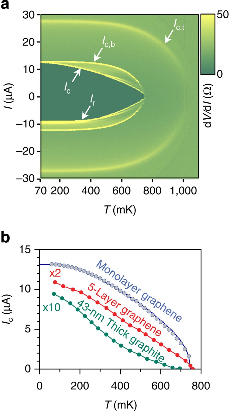
Much efforts have been made for the realization of hybrid Josephson junctions incorporating various materials for the fundamental studies of exotic physical phenomena as well as the applications to superconducting quantum devices. Nonetheless, the efforts have been hindered by the diffusive nature of the conducting channels and interfaces. To overcome the obstacles, we vertically sandwiched a cleaved graphene monoatomic layer as the normal-conducting spacer between superconducting electrodes. The atomically thin single-crystalline graphene layer serves as an ultimately short conducting channel, with highly transparent interfaces with superconductors. In particular, we show the strong Josephson coupling reaching the theoretical limit, the convex-shaped temperature dependence of the Josephson critical current and the exceptionally skewed phase dependence of the Josephson current; all demonstrate the bona fide short and ballistic Josephson nature. This vertical stacking scheme for extremely thin transparent spacers would open a new pathway for exploring the exotic coherence phenomena occurring on an atomic scale.


Figures

Figure 1
Figure 1. Vertical graphene Josephson junction.
(a) In a planar-junction geometry, the reduction of the junction length, L, is limited by the roughness of the electrode edges. (b) In a vertical-junction geometry, L is replaced by the thickness of a single graphene layer, even with rough electrode edges. (c) Scanning electron microscopy image of four nominally identical vertical graphene Josephson junctions (vGJJs). The behaviour of the junction JJ2 was described in detail in the text; MAR was measured in the other junctions (JJ1 and JJ3) to estimate superconducting gap. Monolayer graphene, whose boundary is denoted by a green-dashed line, is sandwiched between the top and bottom Ti/Al/Au superconducting electrodes. In a four-probe measurement setup, the current was biased between I+ and I−, along with simultaneous measurements of the voltage drop between V+ and V−. Scale bar, 5 μm. (d) High-resolution bright-field spherical-aberration-corrected scanning transmission electron microscopy (STEM) image of the cross-section of a vGJJ. The monolayer graphene sheet was atomically in contact with the titanium layer. The highest-intensity peak at the interface corresponded to a width of ~0.44±0.01 nm, which was identical to the thickness of monolayer graphene. Scale bar, 5 nm. (e) Electron energy loss spectroscopy image of the same area as the STEM image in d. Red (yellow) colour denotes the titanium (carbon) element. The monolayer graphene consisting of carbon atoms was sandwiched by two 8-nm-thick titanium adhesion layers. Scale bar, 5 nm.
Figure 2
Figure 2. Josephson coupling through graphene.
(a) Current–voltage (I–V) characteristics of the junction JJ2, measured at the base temperature of 50 mK with a current sweep from negative to positive (blue dots) and vice versa (red dots), exhibited hysteretic behaviour, which may have been of thermal origin. Critical currents of the JJ (Ic), the bottom electrode (Ic,b), the top electrode (Ic,t) and the retrapping current (Ir) are denoted by arrows. Ic and Ic,b coincide with each other at the base temperature. (Inset) I–V characteristics using an expanded scale show the critical current of the top electrode (Ic,t), above which the I–V characteristics exhibited linear behaviour, represented by the red line passing through the origin with normal-state resistance, RN. Ic,b and Ic,t may have been decreased by self-heating in the junction, because they appeared after the JJ switched to the resistive state, whereas Ic itself was free from self-heating. (b) Shapiro steps under microwave exposure of frequency fmw=17 GHz and amplitude P1/2=1.8 (a.u.), occurring in steps of 35.8 μV. (c) Measured ΔV under microwaves of various fmw (symbols) showed good agreement with the ac Josephson relation of ΔV=(h/2e)fmw (line). (d) Colour-coded plot of dV/dI as a function of the bias current and P1/2 at a fixed frequency of fmw=17 GHz; higher-order Shapiro steps were observed.
Figure 3
Figure 3. Temperature dependence of the junction critical current.
(a) Colour-coded plot of dV/dI, measured with a current sweep from negative to positive as a function of temperature T. Tc,b(t) was determined as the temperature where the critical current Ic,b(t) vanished at the interface between the bottom (top) electrode and graphene. Above the critical temperatures of Tc,b and Tc,t at the bottom and top electrodes, respectively, dV/dI became equal to the normal-state resistance, RN. (b) Experimentally measured Ic (blue symbols) of monolayer graphene vGJJ (JJ2), along with the best-fit curve to the short ballistic junction characters (blue line). Temperature dependences of Ic for vGJJs made of five-layer graphene (red symbols) and 43-nm-thick graphite (green symbols). Lines are provided as guides.
Figure 4
Figure 4. Measurements of the current-phase relation.
(a) Schematic diagram of a dc-superconducting quantum interference device (SQUID) containing a tJJ of phase difference γ and a vGJJ of phase difference δ in a superconducting loop. (b) Optical micrograph from the SQUID interferometer used in this study. The tJJ and monolayer graphene are denoted by black- and red-dotted lines, respectively. Scale bar, 5 μm. (c) A highly skewed CPR for an ideal short ballistic JJ with τ=1 (δmax=π; red line), a skewed CPR for a short diffusive JJ (δmax=0.63π; blue line), and a sinusoidal CPR for tJJs with τ=0 (δmax=π/2; green line). δmax, denoted by an arrow for each case, represents the phase difference at which IJ is maximized. (d) Experimentally measured magnetic field dependence of the critical current of the SQUID at the base temperature, Ic,SQ (symbols), was in very good agreement with the expected variation calculated by the short ballistic theory of a JJ (red line) with fitting parameter τ=0.99. The theory for a short diffusive JJ (blue line) cannot account for the highly skewed experimental data.
Figure 5
Figure 5. Calculation of interfacial potential barriers.
(Upper panels) Electrostatic potential ‹V›(z) averaged over the xy plane (a) for graphene (G)/titanium (Ti)/aluminium(Al), and (b) for G/Al. The Fermi level is adjusted to zero. (Lower panels) Atomic structure of G (yellow)/Ti (blue)/Al (purple). (c) ‹V›(z) at Ti/G/Ti structure with varying distance between G and Ti layers (upper panel) for Δd=0–1.0 Å in steps of 0.1 Å and (lower panel) for Δd=1.0~5.0 Å in steps of 0.5 Å. (d) Numerical calculations of quantum tunnelling probability P through the potential barrier at G/Ti interface as a function of Δd. Red dashed line represents P through the potential barrier of direct interface between G and Al layer.
Figure 6
Figure 6. Vertical graphene Josephson junctions with and without graphene insertion.
(a) Optical image of vGJJ devices with graphene (JJwG) and without graphene (JJwoG). Bottom electrode looks brighter than yellowish-coloured top electrode. Scale bar, 10 μm. (b) I-V curves of the JJwG at various temperatures and the schematic of JJwG. (c) I-V curves of the JJwoG show an insulating behaviour similar to those of a superconductor–insulator–superconductor junction with the Josephson current completely suppressed. Schematic structure of JJwoG is shown.
Figure 7
Figure 7. Titanium-based vertical junction.
(a) Optical image of Ti-vJ device is denoted by an arrow. Red dotted line outlines the region of few-layer graphene. Scale bar, 10 μm. (b) Current–voltage (IV) curves of the Ti-vJ measured in zero magnetic field, B (black curve), and B=150 G, which is larger than the critical magnetic field of aluminium, Bc (red curve). Schematic structure of Ti-vJ is shown on the right panel.
Figure 8
Figure 8. Proximity-induced superconducting gap.
(a) Proximity-induced superconducting gap, Δind, is denoted by the red dashed line for aluminium (Al)/titanium (Ti)/Al JJ. L is the junction length between the two Al layers. (b) Normalized LDOS at the centre of Ti layer calculated for the structure of a. Inset, L dependence of ΔTi=Δind (0). Black and red arrows indicate the case of L=16 and 70 nm, respectively. (c) Schematic configuration of a vGJJ and Δind (red dashed line).
Figure 9
Figure 9. Multiple Andreev reflection.
Differential conductance (dI/dV) measured at the base temperature, for JJ1 (a) and for JJ3 (b). MAR peaks are denoted by arrows. The Josephson critical current of each junction is Ic,JJ1=0.53 μA and Ic,JJ3=0.19 μA. The differential conductance map corresponding to the MAR as a function of temperature and the bias voltage, for JJ1 (c) and for JJ3 (d) along with the BCS-type temperature dependence of the gap voltages denoted by dotted lines.

References

    1. Likharev K. K. Superconducting weak links. Rev. Mod. Phys. 51, 101–159 (1979).
    1. Tinkham M. Introduction to Superconductivity Dover (2004).
    1. Doh Y.-J. et al. Tunable supercurrent through semiconductor nanowires. Science 309, 272–275 (2005). - PubMed
    1. Jarillo-Herrero P., van Dam J. A. & Kouwenhoven L. P. Quantum supercurrent transistors in carbon nanotubes. Nature 439, 953–956 (2006). - PubMed
    1. Heersche H. B., Jarillo-Herrero P., Oostinga J. B., Vandersypen L. M. K. & Morpurgo A. F. Bipolar supercurrent in graphene. Nature 446, 56–59 (2007). - PubMed

Publication types

LinkOut - more resources