. 2015 Mar 11:5:8979.
doi: 10.1038/srep08979.

Hall and field-effect mobilities in few layered p-WSe₂ field-effect transistors

Affiliations

Hall and field-effect mobilities in few layered p-WSe₂ field-effect transistors

N R Pradhan et al. Sci Rep. .

Abstract

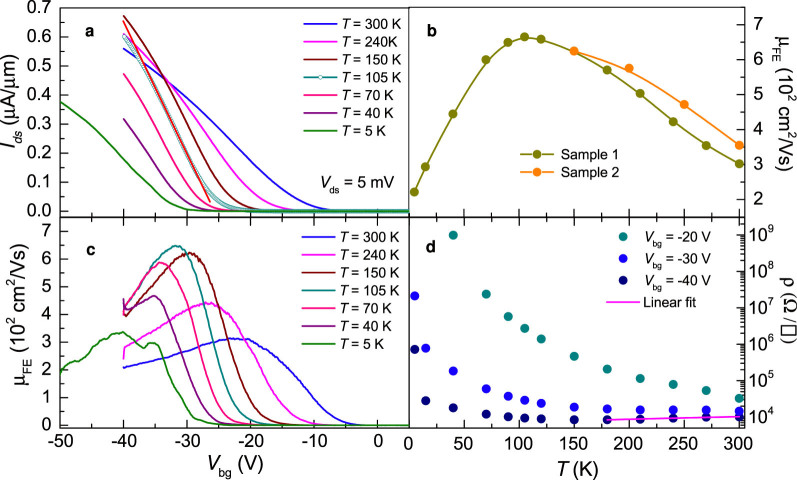
Here, we present a temperature (T) dependent comparison between field-effect and Hall mobilities in field-effect transistors based on few-layered WSe2 exfoliated onto SiO2. Without dielectric engineering and beyond a T-dependent threshold gate-voltage, we observe maximum hole mobilities approaching 350 cm(2)/Vs at T = 300 K. The hole Hall mobility reaches a maximum value of 650 cm(2)/Vs as T is lowered below ~150 K, indicating that insofar WSe2-based field-effect transistors (FETs) display the largest Hall mobilities among the transition metal dichalcogenides. The gate capacitance, as extracted from the Hall-effect, reveals the presence of spurious charges in the channel, while the two-terminal sheet resistivity displays two-dimensional variable-range hopping behavior, indicating carrier localization induced by disorder at the interface between WSe2 and SiO2. We argue that improvements in the fabrication protocols as, for example, the use of a substrate free of dangling bonds are likely to produce WSe2-based FETs displaying higher room temperature mobilities, i.e. approaching those of p-doped Si, which would make it a suitable candidate for high performance opto-electronics.


Figures

Figure 1
Figure 1
(a) Micrograph of the one of our WSe2 field-effect transistors on a 270 nm thick SiO2 layer on p-doped Si. Contacts, (Ti/Au) used to inject the electrical current (Ids), are indicated through labels I+ (source) and I (drain), while the resistivity of the device ρxx was measured through either the pair of voltage contacts labeled as 1 and 2 or pair 3 and 4. The Hall resistance Rxy was measured with an AC excitation either through the pair of contacts 1 and 3 or 2 and 4. Length l of the channel, or the separation between the current contacts, is l = 15.8 μm while the width of the channel is w = 7.7 μm. (b) Height profile (along the blue line shown in the inset) indicating a thickness of 80 Å, or approximately 12 atomic layers for the crystal in (a). Inset: atomic force microscopy image collected from a lateral edge of the WSe2 crystal in (a). (c) Side view sketch of our field-effect transistor(s), indicating that the Ti/Au pads contact all atomic layers, and of the experimental configuration of measurements. (d) Room temperature field-effect mobility μFE as a function of crystal thickness extracted from several FETs based on WSe2 exfoliated onto SiO2. The maximum mobility is observed for ~12 atomic layers.
Figure 2
Figure 2
(a) Current Ids in a logarithmic scale as extracted from a WSe2 FET at T = 300 K and as a function of the gate voltage Vbg for several values of the voltage Vds, i.e. respectively 5 (dark blue line), 26 (red), 47 (blue), 68 (magenta), and 90 mV (brown), between drain and source contacts. Notice that the ON/OFF ratio approaches 106 and subthreshold swing SS ~250 mV per decade. We evaluated the resistance Rc of the contacts by performing also 4 terminal measurements (see Fig. 7 a below) through Rc = Vds/Ids – ρxx l/w, where ρxx is the sheet resistivity of the channel measured in a four-terminal configuration. We found the ratio Rcxx ≈ 20 to remain nearly constant as a function of Vbg. (b) Conductivity σ = S l/w, where the conductance S = Ids/Vds (from (a)), as a function of Vbg and for several values of Vds. Notice, how all the curves collapse on a single curve, indicating linear dependence on Vds. As argued below, this linear dependence most likely results from thermionic emission across the Schottky-barrier at the level of the contacts. (c) Field effect mobility μFE = (1/cg dσ/dVbg as a function of Vbg, where cg = εrε0/d = 12.789 × 10⁻⁹ F/cm2 (for a d = 270 nm thick SiO2 layer). (d) Ids as a function of Vbg, when using an excitation voltage Vds = 5 mV. Red line is a linear fit whose slope yields a field-effect mobility μFE ≈ 300 cm2/Vs.
Figure 3
Figure 3
(a) Current Ids in a logarithmic scale as extracted from the same WSe2 FET in Fig. 2 at T = 105 K and as a function of the gate voltage Vbg for several values of the voltage Vds, i.e. respectively 5 (dark blue line), 26 (red), 47 (magenta), 68 (dark yellow), and 90 mV (brown). Notice that the ON/OFF ratio still approaches 106. (b) Conductivity σ as a function of Vbg for several values of Vds. Notice that even at lower Ts all the curves collapse on a single curve. Notice how the threshold gate voltage Vtbg for conduction increases from ~0 V at 300 K to ~15 V at 105 K. Below, we argue that the observation of, and the increase of Vtbg as T is lowered, corresponds to evidence for charge localization within the channel. (c) Field effect mobility μFE = (1/cg) dσ/dVbg as a function of Vbg. (d) Ids as a function of Vbg, when using an excitation voltage Vds = 5 mV. Red line is a linear fit whose slope yields a field-effect mobility μFE ≈ 665 cm2/Vs.
Figure 4
Figure 4
(a) Ids as a function of the gate voltage Vbg for several temperatures T and for an excitation voltage Vds = 5 mV. From the slopes of the linear fit (red line) one extracts the respective values of the field-effect mobility μFE as a function of the temperature, shown in (b). Orange markers depicts μFE for a second, annealed sample. The field-effect mobility is seen to increase continuously as the temperature is lowered down to T = 105 K, beyond which it decreases sharply. (c) μFE = (1/cg) dσ/dVbg as extracted from the curves in (a). Notice that μFE still saturates at a value of ≈ 300 cm2/Vs at T = 5 K. d Resistivity ρ = 1/σ as a function of T for 3 values of the gate voltage, i.e. −20, −30 and −40 V, respectively (as extracted from the data in (a) or (c)). Magenta line corresponds to a linear fit, describing the behavior of the metallic resistivity, defined by ∂ρ/∂T > 0, observed at higher temperatures when Vbg = −40 V.
Figure 5
Figure 5
Conductivity, i.e. σ = 1/ρ (from the data in Fig. 4 d, acquired under Vds = 5 mV) in a logarithmic scale as a function of T−1/3. Red lines are linear fits, indicating that at lower Ts and for gate voltages below a temperature dependent threshold value Vtbg(T), σ(T) follows the dependence expected for two-dimensional variable-range hopping.
Figure 6
Figure 6
Top panel: Drain to source current Ids as a function of (kBT/e)−1 for several values of the gate voltage Vbg (from the data in Fig. 4a). Red lines are linear fits from which we extract the value of the Schottky energy barrier ϕSB. Bottom panel: ϕSB in a logarithmic scale as a function of Vbg. Red line is a linear fit. The deviation from linearity indicates when the gate voltage matches the flat band condition from which we extract the size of the Schottky barrier Φ ≈ 16 meV.
Figure 7
Figure 7
(a) Four-terminal sheet resistance Rxx measured at a temperature of T = 300 K and as a function of Vbg for a second multilayered WSe2 FET after annealing it under vacuum for 24 h. (b) Hall response Rxy = VH(H)/Ids as a function of the external magnetic field H, and for several values of the gate voltage Vbg. Red lines are linear fits from whose slope we extract the values of the Hall constant RH( = VH/HIds). (c) Density of carriers nH = 1/(eRH) induced by the back gate voltage as a function of Vbg. Red lines are linear fits from which, by comparing the resulting slope σ = n/Vbg = cg*/e (cg* is the effective gate capacitance). (d) Field-effect μFE (magenta and blue lines) and Hall μH = RHxx (red markers) mobilities (where ρxx = Rxxw/l, w and l are the width and the length of the channel, respectively) as functions of Vbg at T = 300 K. (e) Extracted Hall mobility μH as a function of T and for several values of Vbg. μH increases as T is lowered, but subsequently it is seen to decrease below a Vbg -dependent T. (f) Ratio between experimentally extracted and the ideal, or geometrical gate capacitances cg*/cg (black markers) and the mobilities μi = cg*/cg μH (Vbg = −60 V) (red markers) as functions of T. μi are the mobility values that one would obtain if the gate capacitance displayed its ideal cg value in absence of spurious charges in the channel.

References

    1. Wang Q. H., Kalantar-Zadeh K., Kis A., Coleman J. N. & Strano M. S. Electronics and Optoelectronics of Two-Dimensional Transition Metal Dichalcogenides. Nat. Nanotechnol. 7, 699 (2014). - PubMed
    1. Chhowalla M. et al. The Chemistry of Two-Dimensional Layered Transition Metal Dichalcogenide Nanosheets. Nat. Chem. 5, 263–275 (2013). - PubMed
    1. Zeng H. L., Dai J. F., Yao W., Xiao D. & Cui X. D. Valley Polarization in MoS2 Monolayers by Optical Pumping. Nat. Nanotechnol. 7, 490–493 (2012). - PubMed
    1. Mak K. F., He K. L., Shan J. & Heinz T. F. Control of Valley Polarization in Monolayer MoS2 by Optical Helicity. Nat. Nanotechnol. 7, 494–498 (2012). - PubMed
    1. Kim S. et al. High-Mobility and Low-Power Thin-Film Transistors Based on Multilayer MoS2 Crystals. Nat. Commun. 3, 1011 (2012). - PubMed

Publication types