. 2015 Apr 14;112(15):4523-30.
doi: 10.1073/pnas.1416581112. Epub 2015 Mar 27.

The renaissance of black phosphorus

Affiliations

The renaissance of black phosphorus

Xi Ling et al. Proc Natl Acad Sci U S A. .

Abstract

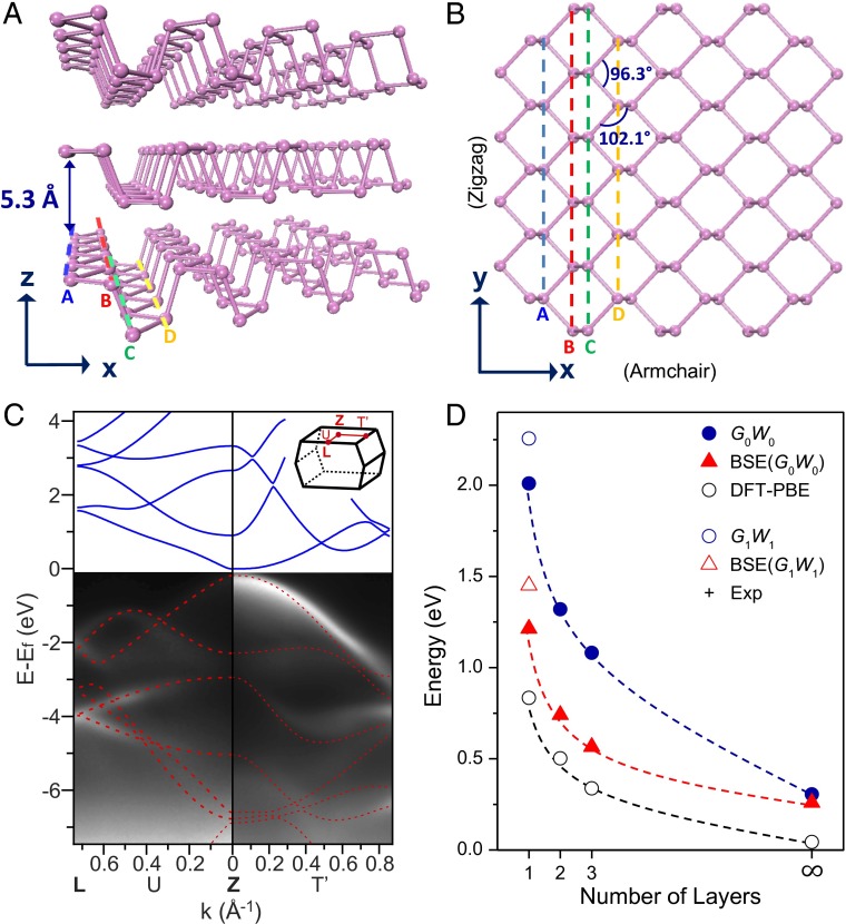
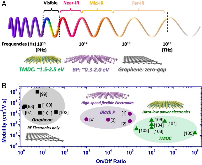
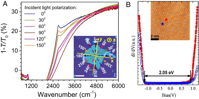
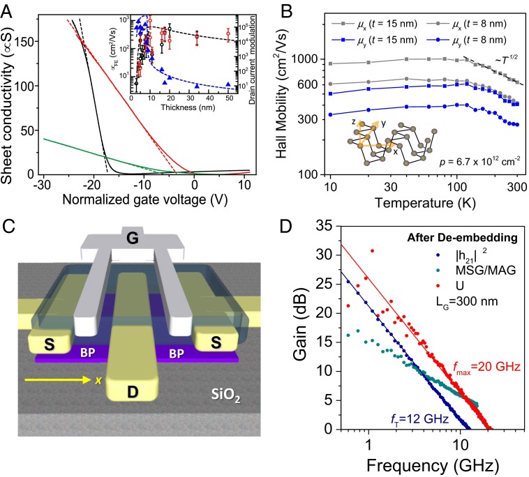
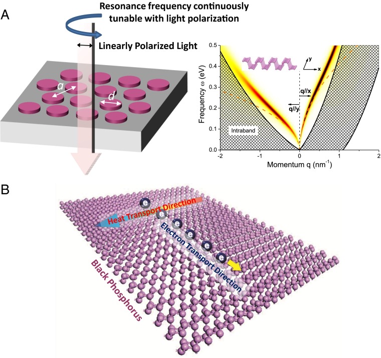
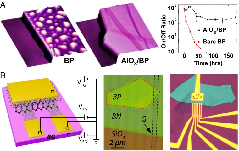
One hundred years after its first successful synthesis in the bulk form in 1914, black phosphorus (black P) was recently rediscovered from the perspective of a 2D layered material, attracting tremendous interest from condensed matter physicists, chemists, semiconductor device engineers, and material scientists. Similar to graphite and transition metal dichalcogenides (TMDs), black P has a layered structure but with a unique puckered single-layer geometry. Because the direct electronic band gap of thin film black P can be varied from 0.3 eV to around 2 eV, depending on its film thickness, and because of its high carrier mobility and anisotropic in-plane properties, black P is promising for novel applications in nanoelectronics and nanophotonics different from graphene and TMDs. Black P as a nanomaterial has already attracted much attention from researchers within the past year. Here, we offer our opinions on this emerging material with the goal of motivating and inspiring fellow researchers in the 2D materials community and the broad readership of PNAS to discuss and contribute to this exciting new field. We also give our perspectives on future 2D and thin film black P research directions, aiming to assist researchers coming from a variety of disciplines who are desirous of working in this exciting research field.

Keywords: 2D material; anisotropic; black phosphorus; nanoelectronic; optoelectronic.


Conflict of interest statement

The authors declare no conflict of interest.

Figures

Fig. 1.
Fig. 1.
Crystal structure and band structure of black P. (A) Side view of the black P crystal lattice. The interlayer spacing is 0.53 nm. (B) Top view of the lattice of single-layer black P. The bond angles are shown. The corresponding x, y, and z directions are indicated in both A and B. x and y correspond to the armchair and zigzag directions of black P, respectively. (C) Band structure of bulk black P mapped out by ARPES measurements. A band gap around 0.3 eV is clearly observed. Superimposed on top are the calculated bands of the bulk crystal. Blue solid and red dashed lines denote empty and filled bands, respectively. The directions of the ARPES mapping are along U (L–Z) and T′, as indicated in the first Brillion zone shown in Inset. Ef is the Fermi energy (1). (D) The evolution of the band gap calculated by different methods, and the energy of the optical absorption peak according to the stacking layer number of few-layer black P (31). C and D are reproduced with permission from refs. and , respectively.
Fig. 2.
Fig. 2.
Electromagnetic wave spectrum and mobility/on–off ratio spectrum. (A) The electromagnetic wave spectrum and the band gap ranges of various types of 2D materials. The frequency ranges corresponding to the band gaps of 2D materials and their applications in optoelectronics are also indicated (96). (B) the “electronics spectrum,” i.e., the mobility/on–off ratio spectrum, of nanomaterials with corresponding performance regions indicated for graphene (–102) (black squares and gray shaded area), black P (–4) (purple dots and light purple shaded area), and TMD [MoS2 (–105), WSe2 (106, 107), and WS2 (108)] (green triangles and light green shaded area) transistors. The dots correspond to data from specific references indicated next to them. The shaded regions are the approximate possible ranges of performance reported for the respective materials in the literature.
Fig. 3.
Fig. 3.
Band gap of thin film and monolayer black P. (A) Polarization-resolved infrared relative extinction spectra of a black P thin film when light is polarized along the six directions, as shown in Inset (an optical micrograph of a black P flake with a thickness of around 30 nm). (Scale bar, 20 μm.) (B) Two representative tunneling spectra plotted on a log scale and measured on a black P surface, showing a wide band gap with an estimated size of 2.05 eV. Inset shows high-resolution STM image (Vbias = +1.2 V, Iset = 150 pA) with a scan size of 2.4 × 3.6 nm. A and B are reproduced with permission from refs. and , respectively.
Fig. 4.
Fig. 4.
Electronic properties of black P thin film. (A) Sheet conductivity measured as a function of gate voltage for devices with different thicknesses: 10 nm (black solid line), 8 nm (red solid line), and 5 nm (green solid line), with field-effect mobility values of 984 cm2⋅V−1⋅s−1, 197 cm2⋅V−1⋅s−1, and 55 cm2⋅V−1⋅s−1, respectively. (Inset) Field-effect mobilities were extracted from the line fit of the linear region of the conductivity (dashed lines). A is reproduced with permission from ref. . (B) Angle-resolved Hall mobility vs. temperature. (Inset) Schematic view of a single-layer black P showing different crystalline directions. B is reproduced with permission from ref. . (C) Schematic of the black P transistor device structure. (D) Current and power gain in black P transistors at gigahertz frequency. Shown are the short-circuit current gain h21, maximum stable gain (MSG)/maximum available gain (MAG), and unilateral power gain U of the 300-nm channel length device after de-embedding. C and D are reproduced with permission from ref. .
Fig. 5.
Fig. 5.
Anisotropic properties of black P for plasmonics and thermoelectrics applications. (A) Schematics of black P-based plasmonic devices with intrinsic anisotropy in their resonance frequency. (Right) The calculated plasmonic dispersions along both the x and y directions of a black P crystal (adopted and modified from ref. 83). (B) Schematics showing the orthogonality between the dominant heat and electron transport directions in single-layer black P, as reported in ref. (inspired by a similar drawing in ref. 69).
Fig. 6.
Fig. 6.
Protective encapsulation of black P material and devices. (A) AFM images and on–off ratio of black P thin film FETs without and with AlOx overlayer protection vs. ambient exposure time. A is reproduced with permission from ref. . (B) Schematic and optical micrograph of a graphene-contacted black P device with boron nitride encapsulation. Red and black dashed areas (Center) show the black phosphorus crystal and one of the graphene strips, respectively. The BN encapsulation layer is also shown. B is reproduced with permission from ref. .

References

    1. Li L, et al. Black phosphorus field-effect transistors. Nat Nanotechnol. 2014;9(5):372–377. - PubMed
    1. Xia F, Wang H, Jia Y. Rediscovering black phosphorus as an anisotropic layered material for optoelectronics and electronics. Nat Commun. 2014;5:4458. - PubMed
    1. Liu H, et al. Phosphorene: An unexplored 2D semiconductor with a high hole mobility. ACS Nano. 2014;8(4):4033–4041. - PubMed
    1. Koenig SP, Doganov RA, Schmidt H, Neto AHC, Özyilmaz B. Electric field effect in ultrathin black phosphorus. Appl Phys Lett. 2014;104(10):103106.
    1. Rodin AS, Carvalho A, Castro Neto AH. Strain-induced gap modification in black phosphorus. Phys Rev Lett. 2014;112(17):176801. - PubMed

Publication types