. 2015 Feb 13:10:67.
doi: 10.1186/s11671-015-0779-5. eCollection 2015.

Dynamics of mass transport during nanohole drilling by local droplet etching

Affiliations

Dynamics of mass transport during nanohole drilling by local droplet etching

Christian Heyn et al. Nanoscale Res Lett. .

Abstract

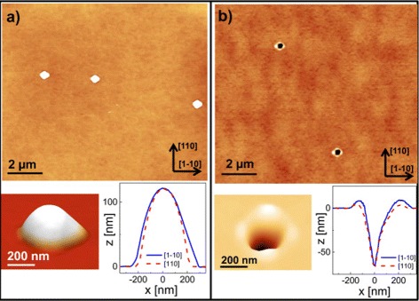
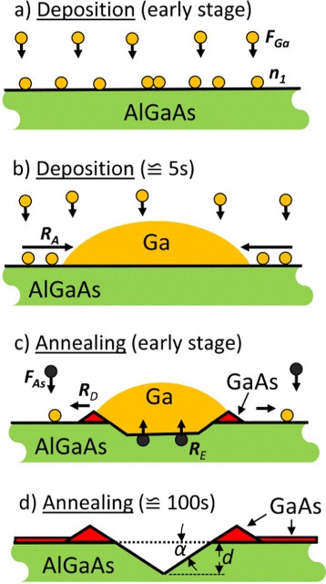
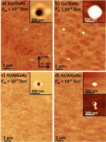
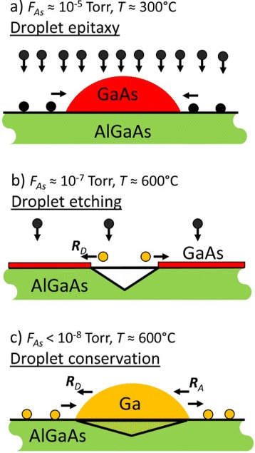
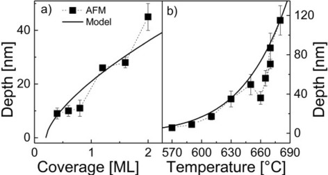
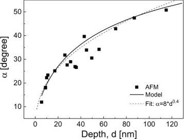
Local droplet etching (LDE) utilizes metal droplets during molecular beam epitaxy for the self-assembled drilling of nanoholes into III/V semiconductor surfaces. An essential process during LDE is the removal of the deposited droplet material from its initial position during post-growth annealing. This paper studies the droplet material removal experimentally and discusses the results in terms of a simple model. The first set of experiments demonstrates that the droplet material is removed by detachment of atoms and spreading over the substrate surface. Further experiments establish that droplet etching requires a small arsenic background pressure to inhibit re-attachment of the detached atoms. Surfaces processed under completely minimized As pressure show no hole formation but instead a conservation of the initial droplets. Under consideration of these results, a simple kinetic scaling model of the etching process is proposed that quantitatively reproduces experimental data on the hole depth as a function of the process temperature and deposited amount of droplet material. Furthermore, the depth dependence of the hole side-facet angle is analyzed.

Keywords: Droplet epitaxy; Droplet etching; Growth modelling; Mass transport; Nanoholes; Self-assembly; Semiconductor nanostructures.


Figures

Figure 1
Figure 1
Example for the transformation of as-grown droplets into nanoholes with walls during post-growth annealing. (a) AFM micrograph of a GaAs surface with droplets after deposition of 2.0 ML of Ga at T=650°C without annealing together with a perspective view and linescans of a single droplet. (b) GaAs surface with nanoholes after Ga droplet deposition and 120-s annealing.
Figure 2
Figure 2
Schematic representation of the different steps of a Ga on AlGaAs droplet etching process. (a) Planar deposition of Ga with flux F Ga yielding an increase of the Ga adatom density n 1. Ga droplets are nucleated by collisions between diffusing Ga adatoms. (b) Droplet shape establishment with increasing coverage and increase of the droplet volume by adatom attachment with rate R A. (c) Etching and removal of substrate material by As diffusion with rate R E and droplet material detachment with rate R D during post-growth annealing. The detached Ga atoms crystallize a thin GaAs layer with background As of flux F As. (d) Final hole with depth d and side-facet angle α surrounded by a GaAs wall.
Figure 3
Figure 3
Photoluminescence and transport experiments establishing the droplet material spreading over the surface. (a) Photoluminescence (PL) measurement of a GaAs quantum ring (QR) sample fabricated using Ga LDE. The insert shows a schematic sample cross section. In addition to the weak QR signal, a peak at 1.917 V indicates the presence of a uniform GaAs quantum well (QW) with thickness of 0.85 nm. Importantly, the volume of the additional planar layer agrees with the amount of deposited droplet material. (b) Current density j over a 8-nm-thick AlAs tunnel barrier (reference) compared to a sample, where the tunnel barrier has been thickened by an additional Al-LDE step. The insert shows a schematic sample cross section.
Figure 4
Figure 4
AFM images demonstrating droplet conservation at completely minimized As background. (a) GaAs surface after Ga-LDE with θ = 2.0 ML and T=600°C. The As flux F As during annealing is of about 1 ×10⁻⁷ Torr according to our typical process conditions. (b) GaAs surface after Ga-LDE at minimized As background flux F As<1×10⁻⁸ Torr by a 1-h growth interruption with the As cell switched off before etching. (c) AlGaAs surface after Al-LDE with θ = 1.0 ML, T=640°C, and F As≃1×10⁻⁷ Torr. (d) AlGaAs surface after Al-LDE at F As<1×10⁻⁸ Torr.
Figure 5
Figure 5
Scheme of droplet-epitaxy-based regimes at different As fluxes F As and process temperatures T . (a) Droplet epitaxy with crystallization of GaAs QDs using a high F As. (b) Droplet etching of nanoholes at high T and small F As. Here, Ga atoms detaching from the droplet crystallize with background As and form a thin GaAs layer. (c) Droplet conservation at high T and minimized F As. Adatom detachment from and re-attachment to the droplets is balanced.
Figure 6
Figure 6
Measured and calculated depth d of Al droplet etched nanoholes. (a) Comparison of measured and calculated depth d of Al-droplet-etched nanoholes as a function of the Al coverage θ. The model results (line) are calculated using Equation 3, and the experimental data (symbols) are taken from [47]. (b) Measured and calculated depth d of Al-droplet-etched nanoholes as a function of the process temperature T.
Figure 7
Figure 7
Measured and calculated hole side-facet angle α as function of the hole depth. Every data point represents the average over a sample with d varied by changing T and θ. In addition to calculations done using a model described in [47], results of a simple power-law fit are shown.

References

    1. Moison JM, Houzay F, Barthe F, Leprince L, André E, Vatel O. Selforganized growth of regular nanometerscale InAs dots on GaAs. Appl Phys Lett. 1994;64(2):196–8. doi: 10.1063/1.111502. - DOI
    1. Madhukar A, Xie Q, Chen P, Konkar A. Nature of strained InAs threedimensional island formation and distribution on GaAs (100) Appl Phys Lett. 1994;64(20):2727–9. doi: 10.1063/1.111456. - DOI
    1. Leonard D, Krishnamurthy M, Fafard S, Merz JL, Petroff PM. Molecular beam epitaxy growth of quantum dots from strained coherent uniform islands of InGaAs on GaAs. J Vacuum Sci Technol B. 1994;12(2):1063–6. doi: 10.1116/1.587088. - DOI
    1. Mo YW, Savage DE, Schwartzentruber BS, Lagally MG. Kinetic pathway in Stranski-Krastanov growth of Ge on Si(001) Phys Rev Lett. 1990;65(8):1020–3. doi: 10.1103/PhysRevLett.65.1020. - DOI - PubMed
    1. Chikyow T, Koguchi N. MBE growth method for pyramid-shaped GaAs micro crystals on ZnSe (001) surface using Ga droplets. Jpn J Appl Phys. 1990;29(Part 2, No. 11):2093–5. doi: 10.1143/JJAP.29.L2093. - DOI

LinkOut - more resources