

Structural and optical properties of position-retrievable low-density GaAs droplet epitaxial quantum dots for application to single photon sources with plasmonic optical coupling
- PMID: 25852409
- PMCID: PMC4385222
- DOI: 10.1186/s11671-015-0826-2
Structural and optical properties of position-retrievable low-density GaAs droplet epitaxial quantum dots for application to single photon sources with plasmonic optical coupling
Abstract
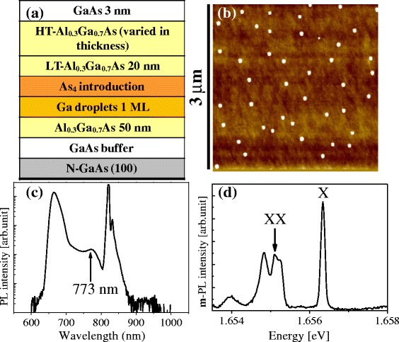
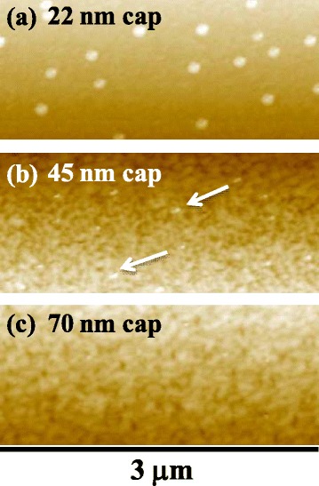
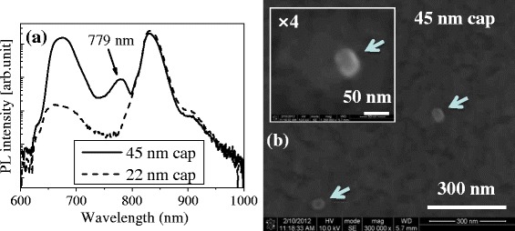
The position of a single GaAs quantum dot (QD), which is optically active, grown by low-density droplet epitaxy (DE) (approximately 4 QDs/μm(2)), was directly observed on the surface of a 45-nm-thick Al0.3Ga0.7As capping layer. The thin thickness of AlGaAs capping layer is useful for single photon sources with plasmonic optical coupling. A micro-photoluminescence for GaAs DE QDs has shown exciton/biexciton behavior in the range of 1.654 to 1.657 eV. The direct observation of positions of low-density GaAs DE QDs would be advantageous for mass fabrication of devices that use a single QD, such as single photon sources.
Keywords: Droplet epitaxy; GaAs; Micro-photoluminescence; Quantum dot; Single photon.
Figures
References
-
- Cavigli L, Abbarchi M, Bietti S, Somaschini C, Sanguinetti S, Koguchi N, et al. Individual GaAs quantum emitters grown on Ge substrates. Appl Phys Lett. 2011;98:103104. doi: 10.1063/1.3560303. - DOI
-
- Jo M, Mano T, Sakoda K. Two-step formation of gallium droplets with high controllability of size and density. Cryst Growth Des. 2011;11:4647. doi: 10.1021/cg200930v. - DOI
-
- Liang BL, Wang Zh M, Lee JH, Sablon K, Mazur Yu I, Salamo GJ. Low density InAs quantum dots grown on GaAs nanoholes. Appl Phys Lett. 2006;89:043113. doi: 10.1063/1.2244043. - DOI
-
- Ishikawa T, Nishimura T, Kohmoto S, Asakawa K. Site-controlled InAs single quantum-dot structures on GaAs surfaces patterned by in situ electron-beam lithography. Appl Phys Lett. 2000;76:167. doi: 10.1063/1.125691. - DOI
LinkOut - more resources
Full Text Sources
Other Literature Sources
