

Comment
doi: 10.1021/acsnano.5b01762.
Epub 2015 Apr 13.
Controlling defects in graphene for optimizing the electrical properties of graphene nanodevices
Affiliations
- PMID: 25864552
- PMCID: PMC4415450
- DOI: 10.1021/acsnano.5b01762
Item in Clipboard
Comment
Controlling defects in graphene for optimizing the electrical properties of graphene nanodevices
ACS Nano.
.
Abstract
Structural defects strongly impact the electrical transport properties of graphene nanostructures. In this Perspective, we give a brief overview of different types of defects in graphene and their effect on transport properties. We discuss recent experimental progress on graphene self-repair of defects, with a focus on in situ transmission electron microscopy studies. Finally, we present the outlook for graphene self-repair and in situ experiments.
Figures
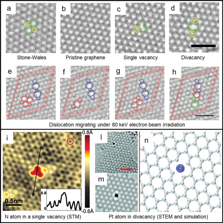
Structural defects in graphene. (a–d) High-resolution transmission electron microscopy (HRTEM) images of (a) Stone–Wales defect, (b) defect-free graphene, (c) single vacancy with 5–9 rings, (d) divacancy with 5–8–5 rings. Scale bar is 1 nm. (e–h) HRTEM image sequence of divacancy migration observed at 80 keV. Scale bar is 1 nm. Reprinted with permission from ref (13). Copyright 2011 American Physical Society. (i) Scanning transmission microscopy image of a single N atom dopant in graphene on a copper foil substrate. (Inset) Line profile across the dopant shows atomic corrugation and apparent height of the dopant. Reprinted with permission from ref (15). Copyright 2011 American Association for the Advancement of Science. (l,m) HRTEM images of a Pt atom trapped in divacancy and (n) simulated HRTEM image for the Pt vacancy complex. Scale bar is 1 nm. Reprinted from ref (14). Copyright 2012 American Chemical Society.
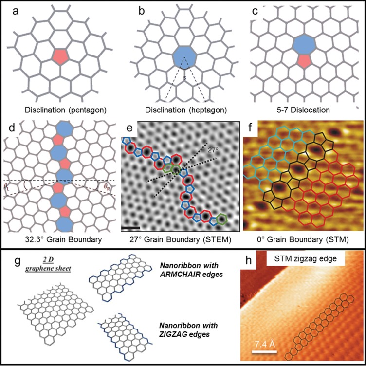
(a–f) Topological defects in graphene. (a,b) 5 ring and 7 ring disclinations, (c) 5–7 dislocation, (d) grain boundary with θ = 32.3° misorientation angle. Reprinted with permission from ref (16). Copyright 2014 Nature Publishing Group. (e) Aberration-corrected annular dark-field scanning transmission electron microscopy (STEM) of a grain boundary with θ = 27° misorientation angle. Scale bar is 0.5 nm. Reprinted with permission from ref (28). Copyright 2011 Nature Publishing Group. (f) Scanning transmission microscopy image of a 0° grain boundary, formed by 5 and 8 carbon atom rings. Reprinted with permission from ref (5). Copyright 2010 Nature Publishing Group. (g) Zigzag and armchair edges in monolayer graphene nanoribbons. Reprinted with permission from ref (20). Copyright 2010 Royal Society of Chemistry. (h) Atomic-resolution STM image of graphene edge structure on the sloped sidewall of SiC. Reprinted with permission from ref (19). Copyright 2014 Nature Publishing Group.
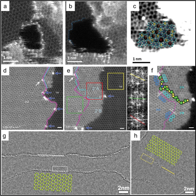
Graphene self-repair experiments. (a–c) Aberration-corrected high-angle annular dark-field scanning transmission electron microscopy (HAADF-STEM) (at 60 keV) images showing (a) a hole etched in graphene that is decorated with Pd atoms, (b) the stabilization of the hole in the absence of Pd atoms at the edge, and (c) the hole refilling with 5, 6, 7, and 8 carbon atom rings. The sample is at room temperature, in ultrahigh vacuum. Reprinted from ref (23). Copyright 2012 American Chemical Society. (d,e) Aberration-corrected HAADF-STEM (at 60 keV) images showing (d) a graphene area which is single layer on the right side and bilayer on the left and (e) the same area after a cumulative electron dose of 3.87 × 10⁹e nm–2. The inset shows the Fourier transform images corresponding to the 1st (yellow box), 2nd (green box), and 2+ (red box) layer of graphene. (f) Detail of the previous image, showing the grain boundary formed between the newly grown graphene (2+A and 2+B) and the original 2nd layer. The sample is heated to 500 °C. Scale bar is 0.5 nm. Reprinted with permission from ref (7). Copyright 2014 Nature Publishing Group. (g,h) High-resolution transmission electron microscopy images of nanoribbons in monolayer graphene sculpted at 300 keV at 600 °C and imaged at 80 keV at 600 °C. The ribbons in (g) and (h) are oriented, respectively, along the ⟨11̅00⟩ and ⟨12̅00⟩ directions. White and yellow lines indicate armchair and zigzag edges, respectively. Atom structure models for armchair and zigzag edges, outlined with open frames in the corresponding images, are enlarged and overlaid. Reprinted from ref (24). Copyright 2013 American Chemical Society.
Comment on
-
Electronic transport of recrystallized freestanding graphene nanoribbons.ACS Nano. 2015;9(4):3510-20. doi: 10.1021/nn507452g. Epub 2015 Mar 9. ACS Nano. 2015. PMID: 25738404
References
-
- Haskins J.; Kınacı A.; Sevik C.; Sevinçli H.; Cuniberti G.; Çağın T. Control of Thermal and Electronic Transport in Defect-Engineered Graphene Nanoribbons. ACS Nano 2011, 5, 3779–3787. - PubMed
-
- Tsen A. W.; Brown L.; Levendorf M. P.; Ghahari F.; Huang P. Y.; Havener R. W.; Ruiz-Vargas C. S.; Muller D. A.; Kim P.; Park J. Tailoring Electrical Transport Across Grain Boundaries in Polycrystalline Graphene. Science 2012, 336, 1143–1146. - PubMed
-
- Stampfer C.; Güttinger J.; Hellmüller S.; Molitor F.; Ensslin K.; Ihn T. Energy Gaps in Etched Graphene Nanoribbons. Phys. Rev. Lett. 2009, 102, 056403. - PubMed
-
- Lherbier A.; Dubois S. M.-M.; Declerck X.; Niquet Y.-M.; Roche S.; Charlier J.-C. Transport Properties of Graphene Containing Structural Defects. Phys. Rev. B 2012, 86, 075402.
-
- Lahiri J.; Lin Y.; Bozkurt P.; Oleynik I. I.; Batzill M. An Extended Defect in Graphene as a Metallic Wire. Nat. Nanotechnol. 2010, 5, 326–329. - PubMed
Publication types
MeSH terms
Substances
LinkOut - more resources
Full Text Sources
Other Literature Sources
