. 2015 May 14:6:7149.
doi: 10.1038/ncomms8149.

Wearable red-green-blue quantum dot light-emitting diode array using high-resolution intaglio transfer printing

Affiliations

Wearable red-green-blue quantum dot light-emitting diode array using high-resolution intaglio transfer printing

Moon Kee Choi et al. Nat Commun. .

Abstract

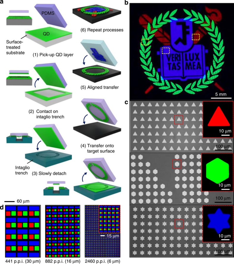
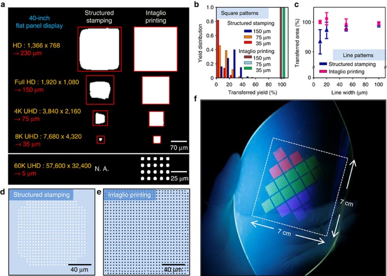
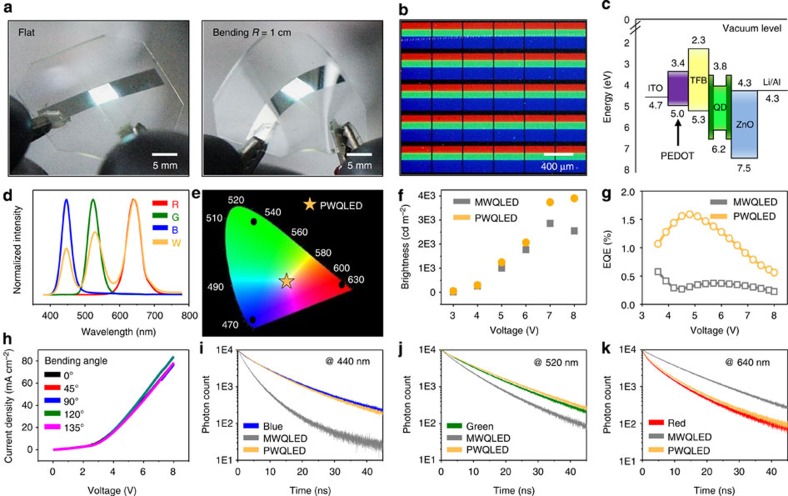
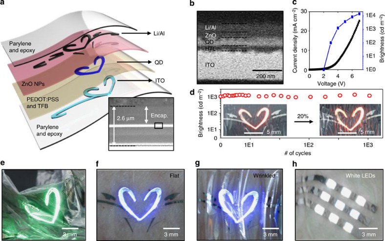
Deformable full-colour light-emitting diodes with ultrafine pixels are essential for wearable electronics, which requires the conformal integration on curvilinear surface as well as retina-like high-definition displays. However, there are remaining challenges in terms of polychromatic configuration, electroluminescence efficiency and/or multidirectional deformability. Here we present ultra-thin, wearable colloidal quantum dot light-emitting diode arrays utilizing the intaglio transfer printing technique, which allows the alignment of red-green-blue pixels with high resolutions up to 2,460 pixels per inch. This technique is readily scalable and adaptable for low-voltage-driven pixelated white quantum dot light-emitting diodes and electronic tattoos, showing the best electroluminescence performance (14,000 cd m(-2) at 7 V) among the wearable light-emitting diodes reported up to date. The device performance is stable on flat, curved and convoluted surfaces under mechanical deformations such as bending, crumpling and wrinkling. These deformable device arrays highlight new possibilities for integrating high-definition full-colour displays in wearable electronics.


Figures

Figure 1
Figure 1. Intaglio transfer printing for high-resolution RGB QLEDs.
(a) Schematic illustration of the intaglio transfer printing process. Inset images on the left of each frame show the side view. (b) The PL image of the RGB QD patterns via multiple aligned transfer printings. (c) Magnified views of selected regions of b. Each colour pattern consists of thousands of tens-of-microns-sized pixels (red: triangle (top), green: hexagon (middle) and blue: star (bottom)). Insets show further magnified PL images of pixels. (d) The PL images showing aligned RGB pixels whose resolution is between 441 p.p.i. (left) and 2,460 p.p.i. (right).
Figure 2
Figure 2. Experimental and theoretical analysis of the intaglio transfer printing.
(a) Pattern size scaling in the structured stamping (left) and intaglio transfer printing (right). QD transfer yields of the structured stamping dramatically decrease especially in high resolutions, while those of the intaglio printing approach ∼100% in all design rules. (b) Distribution of transfer printing yields at different pattern sizes (150, 75 and 45 μm). The transfer printing yield for the structured stamping dramatically decreases with the pattern size, while that of intaglio printing maintains ∼100%. Detailed results are shown in Supplementary Fig. 2. (c) Percentile proportion of the transferred QD line pattern area to the original pattern area. As the line width decreases from 100 to 10 μm, the structured stamping yield decreases, while intaglio printing maintains ∼100%. Detailed results are shown in Supplementary Fig. 4. (d,e) FEM simulations of the transferred area of the rectangular pattern (size: 150 × 150 μm) for the structured stamping (d) and intaglio printing (e). (f) PL image of a large-area QD dot array (7 × 7 cm) patterned by repeated aligned intaglio transfer printing on a flexible polyethylene terephthalate substrate.
Figure 3
Figure 3. True-white light emission based on pixelated RGB QLEDs.
(a) Optical images of the flexible white QLEDs under the bias. (b) Magnified view (PL image) of the RGB QD pixels of white QLEDs. (c) Energy band diagram of white QLEDs estimated by the ultraviolet photoelectron spectrometry. (d) EL spectra of PWQLEDs and each monochromatic (R, G and B) QLED. (e) CIE 1931 xy chromaticity diagram showing the true-white colour (0.39, 0.38) of PWQLEDs. (f) Brightness versus voltage of PWQLEDs and MWQLEDs. PWQLEDs show the higher efficiency than MWQLEDs, particularly at the high brightness. (g) External quantum efficiency of PWQLEDs and MWQLEDs. (h) Electrical properties (J–V characteristics) at different bending angles. (ik) Time-resolved PL spectra of aligned RGB (PWQLED), mixed (MWQLED), and monochromatic (R, G and B) QD layers.
Figure 4
Figure 4. Electronic tattoo demonstrations using ultra-thin wearable QLEDs.
(a) Exploded view of the electronic tattoo, which shows the layer information of the device. The inset is a cross-sectional scanning electron microscope (SEM) image of the electronic tattoo in which the thickness of the encapsulation and active layers are shown. (b) Magnified view of the cross-sectional SEM image (inset of Fig. 4a) that shows the detailed layer information of active layers. (c) The J–V–L characteristics of the ultra-thin, wearable QLEDs. (d) Stable brightness in multiple stretching experiments (∼20%, 1,000 times). The inset shows photographs of buckled and stretched ultra-thin red QLEDs (0 and ∼20%, left and right). (e) Optical image of ultra-thin green QLEDs laminated on crumpled Al foil. (f,g) Photographs of the electronic tattoo (blue QLEDs) laminated on the human skin (f). The wearable QLEDs maintain the original optoelectronic performances even under skin deformations (g). (h) Optical image of wearable PWQLED arrays laminated on the human skin.

References

    1. Xu S. et al.. Soft microfluidic assemblies of sensors, circuits, and radios for the skin. Science 344, 70–74 (2014). - PubMed
    1. Kaltenbrunner M. et al.. An ultra-lightweight design for imperceptible plastic electronics. Nature 499, 458–463 (2013). - PubMed
    1. Son D. et al.. Multifunctional wearable devices for diagnosis and therapy of movement disorders. Nat. Nanotechnol. 9, 397–404 (2014). - PubMed
    1. Lipomi D. J. et al.. Skin-like pressure and strain sensors based on transparent films of carbon nanotubes. Nat. Nanotechnol. 6, 788–792 (2011). - PubMed
    1. Pimputkar S., Speck J. S., Denbaars S. P. & Nakamura S. Prospects for LED lighting. Nat. Photonics 3, 180–182 (2009).

Publication types