

Strain in a silicon-on-insulator nanostructure revealed by 3D x-ray Bragg ptychography
- PMID: 25984829
- PMCID: PMC4434906
- DOI: 10.1038/srep09827
Strain in a silicon-on-insulator nanostructure revealed by 3D x-ray Bragg ptychography
Abstract
Progresses in the design of well-defined electronic band structure and dedicated functionalities rely on the high control of complex architectural device nano-scaled structures. This includes the challenging accurate description of strain fields in crystalline structures, which requires non invasive and three-dimensional (3D) imaging methods. Here, we demonstrate in details how x-ray Bragg ptychography can be used to quantify in 3D a displacement field in a lithographically patterned silicon-on-insulator structure. The image of the crystalline properties, which results from the phase retrieval of a coherent intensity data set, is obtained from a well-controlled optimized process, for which all steps are detailed. These results confirm the promising perspectives of 3D Bragg ptychography for the investigation of complex nano-structured crystals in material science.
Figures
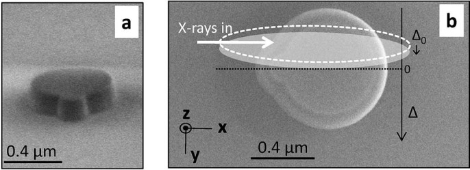
 (black arrow) and the
scanning step
(black arrow) and the
scanning step  are indicated. The
projected direction of propagation of the incident beam (white arrow)
together with the beam footprint (FWHM of intensity, dotted ellipse) are
shown. The gray ellipse corresponds to the beam footprint at the next
beam-to-sample position. The (
are indicated. The
projected direction of propagation of the incident beam (white arrow)
together with the beam footprint (FWHM of intensity, dotted ellipse) are
shown. The gray ellipse corresponds to the beam footprint at the next
beam-to-sample position. The ( orthogonal laboratory frame is given.
 and
to the phase
and
to the phase  , respectively. (c)
Description of the 3D Bragg diffraction geometry, including the Bragg angle
(
, respectively. (c)
Description of the 3D Bragg diffraction geometry, including the Bragg angle
( ), the incident and exit wave
vectors (
), the incident and exit wave
vectors ( , respectively) and the
Bragg vector (
, respectively) and the
Bragg vector ( ). The 3D
non-orthogonal (
). The 3D
non-orthogonal ( ) detection frame
is defined in agreement with the detection acquisition modality,
corresponding to the 2D detector plane and to the rocking curve direction.
The (
) detection frame
is defined in agreement with the detection acquisition modality,
corresponding to the 2D detector plane and to the rocking curve direction.
The ( ) laboratory frame is also
shown.
) laboratory frame is also
shown.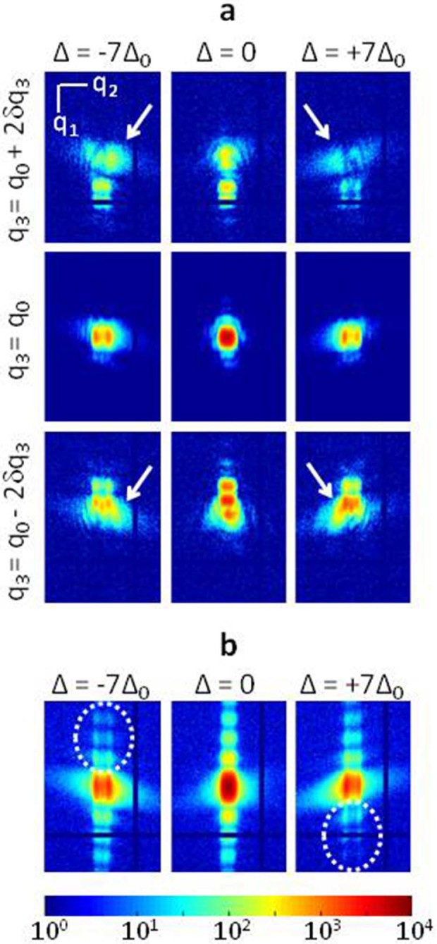
 plane, only the central part of the pattern is
shown. The steps along
plane, only the central part of the pattern is
shown. The steps along  correspond
to
correspond
to  , relatively to the most central
position
, relatively to the most central
position  while along the
ptychography translation
while along the
ptychography translation  , the
steps are
, the
steps are  (
( m−1 and
  nm). The intensity values in
  have been increased by a factor
of 4 for sake of clarity. The white arrows emphasize the stronger intensity
lobes, which are arising from the structure edges. (b) Intensity integrated
along the
have been increased by a factor
of 4 for sake of clarity. The white arrows emphasize the stronger intensity
lobes, which are arising from the structure edges. (b) Intensity integrated
along the  direction, for a fixed
 , identical to (a). The
dotted ellipses emphasize the missing intensity along the vertical streaks.
In (a) and (b), the vertical and horizontal zero intensity lines correspond
to blind pixels in the detector. The common logarithmic photon scale is
shown in (b).
, identical to (a). The
dotted ellipses emphasize the missing intensity along the vertical streaks.
In (a) and (b), the vertical and horizontal zero intensity lines correspond
to blind pixels in the detector. The common logarithmic photon scale is
shown in (b).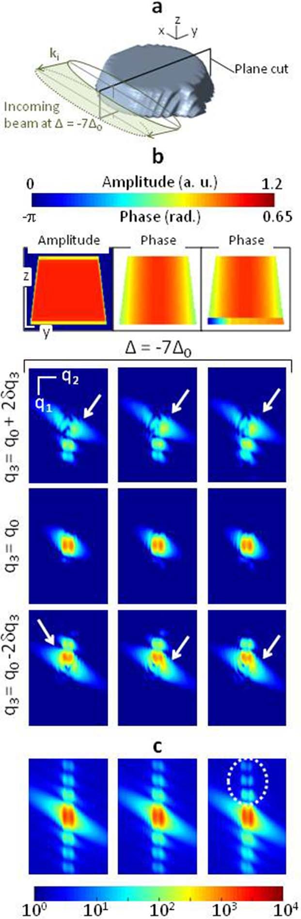
 . The laboratory frame is given; the length of the black lines is
100 nm. (b) Three synthetic models, corresponding to three different strain
states and their corresponding diffraction patterns. The 2D sample
description is shown in the plane indicated in (a) while the diffraction
patterns are taken at the same
. The laboratory frame is given; the length of the black lines is
100 nm. (b) Three synthetic models, corresponding to three different strain
states and their corresponding diffraction patterns. The 2D sample
description is shown in the plane indicated in (a) while the diffraction
patterns are taken at the same  and
and  values as the ones of (Figure 2, left column). (c) Intensity integrated along
the
values as the ones of (Figure 2, left column). (c) Intensity integrated along
the  direction, for the same
  value. The specific features of
the calculated diffraction patterns are emphasized by the white arrows and
the dotted ellipse. The three strain states are as followed: (Left)
The 3D strain-free crystal case. A 2D cut through the 3D amplitude is shown
in (a). Note the assymetry in the spatial scale, which is underlined by the
white lines, representing a 100 nm length. (Middle) Same calculation,
obtained for a strained crystal: a displacement field with a radial symmetry
is introduced at the edge of the structure. A 2D cut through the
corresponding sample phase is shown at the top. (Right) Same as
before with the simultaneous introduction of the displacement field at the
edges and at the interface. This last model produces diffraction patterns in
good agreement with the experimental ones.
value. The specific features of
the calculated diffraction patterns are emphasized by the white arrows and
the dotted ellipse. The three strain states are as followed: (Left)
The 3D strain-free crystal case. A 2D cut through the 3D amplitude is shown
in (a). Note the assymetry in the spatial scale, which is underlined by the
white lines, representing a 100 nm length. (Middle) Same calculation,
obtained for a strained crystal: a displacement field with a radial symmetry
is introduced at the edge of the structure. A 2D cut through the
corresponding sample phase is shown at the top. (Right) Same as
before with the simultaneous introduction of the displacement field at the
edges and at the interface. This last model produces diffraction patterns in
good agreement with the experimental ones.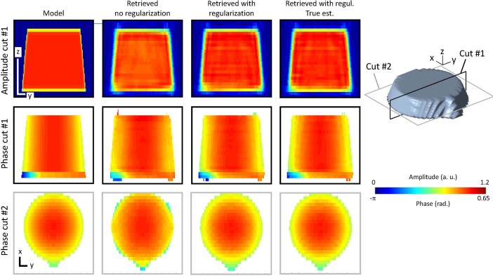
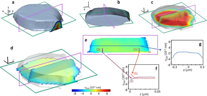
 . The color scale used to plot the
  images is given at the bottom. (e) 2D cut in
the (y,z) plane extracted from (d). The specific behavior of
images is given at the bottom. (e) 2D cut in
the (y,z) plane extracted from (d). The specific behavior of
 is emphasized in the 1D cuts
taken along the colored lines in (f) and (g).
is emphasized in the 1D cuts
taken along the colored lines in (f) and (g).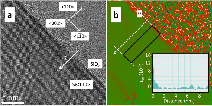
 layer are indicated. (b) The
  strain component extracted from (a),
in absolute units. The inset shows the mean value of
strain component extracted from (a),
in absolute units. The inset shows the mean value of  as a function of the distance to the
interface, calculated in the region delimited by the black rectangle. An
increase of
as a function of the distance to the
interface, calculated in the region delimited by the black rectangle. An
increase of  is observed near the
interface.
is observed near the
interface.References
-
- Bedell S. W., Khakifirooz A., and Sadana D. K. Strain scaling for CMOS. MRS Bulletin 39, 131–137, 2 (2014).
-
- Roberts M. M., et al. Elastically relaxed free-standing strained-silicon nanomembranes. Nat. Mater. 5, 388–393, 2006. - PubMed
-
- Liu J., Sun X., Camacho-Aguilera R., Kimerling L. C., and Michel J. Ge-on-Si laser operating at room temperature. Opt. Lett. 35, 679–681, 2010. - PubMed
-
- Suess M. J., et al. Analysis of enhanced light emission from highly strained germanium microbridges. Nat. Phot. 7, 466 (2013).
-
- Celler G. K., and Cristoloveanu S. Frontiers of silicon-on-insulator. J. Appl. Phys. 93, 4955 (2003).
Publication types
LinkOut - more resources
Full Text Sources
Other Literature Sources
