. 2015 May 26:6:7170.
doi: 10.1038/ncomms8170.

High-performance green flexible electronics based on biodegradable cellulose nanofibril paper

Affiliations

High-performance green flexible electronics based on biodegradable cellulose nanofibril paper

Yei Hwan Jung et al. Nat Commun. .

Abstract

Today's consumer electronics, such as cell phones, tablets and other portable electronic devices, are typically made of non-renewable, non-biodegradable, and sometimes potentially toxic (for example, gallium arsenide) materials. These consumer electronics are frequently upgraded or discarded, leading to serious environmental contamination. Thus, electronic systems consisting of renewable and biodegradable materials and minimal amount of potentially toxic materials are desirable. Here we report high-performance flexible microwave and digital electronics that consume the smallest amount of potentially toxic materials on biobased, biodegradable and flexible cellulose nanofibril papers. Furthermore, we demonstrate gallium arsenide microwave devices, the consumer wireless workhorse, in a transferrable thin-film form. Successful fabrication of key electrical components on the flexible cellulose nanofibril paper with comparable performance to their rigid counterparts and clear demonstration of fungal biodegradation of the cellulose-nanofibril-based electronics suggest that it is feasible to fabricate high-performance flexible electronics using ecofriendly materials.


Figures
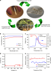
Figure 1
Figure 1. Introduction to cellulose nanofibril (CNF) paper and its basic characteristics as a substrate for electronics.
(a) An illustration of a likely life cycle of the biobased and biodegradable CNF paper. First, cellulose nanofibrils (CNFs) extracted from the woods is made into CNF paper. The CNF paper can be degraded via fungal biodegradation and sent back to the woods without adverse environmental effects. (b) The transmittance curve over a visible spectrum. Blue and red curves show the transmittance of 80-μm and 200-μm thick CNF films, respectively. (c) A thermogravimetric (TGA) plot showing the weight change of the CNF film as a function of temperature, along with the first derivative of the curve. The film remains stable up to 213 °C. (d) The electrical breakdown characteristics of CNF film. Current is measured while high voltage is applied on both sides of the film. (e) Radio frequency characteristics of the CNF film. Dielectric constant (red) and loss tangent (blue) are measured in the frequency range of 0 to 10 GHz using a microstrip waveguide.
Figure 2
Figure 2. The fabrication process for deterministic assembly of GaAs devices on CNF paper and quantitative analysis on the influence of GaAs to the environment.
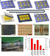
(a) Schematic illustration of the fabrication process of GaInP/GaAs HBTs on a CNF substrate. The HBTs are fabricated on a sacrificial layer grown on a GaAs substrate and released with protective anchors made of photoresists. Each HBT is picked up using a PDMS micro-stamp and printed onto a temporary Si substrate with polyimide as the adhesive. After RF interconnect metallization, the devices are released from the temporary substrate and printed onto a CNF substrate using a PDMS stamp. (b) An optical microscopy image showing 1,500 releasable HBTs in a dense array format on a 5 × 6 mm2 size GaAs substrate. Scale bar, 2 mm. (c) A magnified image of the array. Scale bar, 200 μm. (d) An optical image showing a single releasable HBT that is tethered to the substrate with photoresist anchors. Scale bar, 30 μm. (e) A photograph of an array of HBTs on a CNF substrate wrapped around a tree stick with a ∼3 mm radius. (f) Comparison chart showing the amount of the arsenic corresponding to each type of device/transistor listed as well as the amount of water calculated according to the EPA standard based on the quantity of the arsenic present in these devices/transistors. For a single conventional cell phone, ∼138 l of water is required to satisfy the EPA standard, whereas only 0.32 l is required using our approach. In addition, 23 l is required for a single conventional chip with 40 HBTs, while only 0.054 l is required for the same number of HBTs with our approach. One HBT only requires 0.0013, l of water.
Figure 3
Figure 3. Microwave active GaAs electronic devices on CNF paper.
(a) Photograph of an array of HBTs on a CNF substrate put on a tree leaf. (b) Magnified photograph of the array. (c) Gummel plot and β plot showing the maximum DC gain of the HBT. The maximum β is 14.49. The inset optical image shows one of the HBTs in the array that was measured and characterized. (d) IC versus VCE plot of the HBT plotted at 0.5 mA steps of IB. (e) Current gain (H21) and power gain (GMAX) as a function of frequency, with a collector voltage bias of 2 V and a base current bias of 2 mA. (f) Current versus voltage plot of the Schottky diode on a CNF substrate. The red curve shows the logarithmic scale and the blue curve shows the linear scale. The inset optical image shows the diode transferred onto a CNF substrate with G–S–G interconnects. (g) Measured S11 (red) and S21 (blue) plotted against frequency under a forward current bias of 10 mA. (h) Measured S11 (red) and S21 (blue) plotted against frequency under a reverse voltage bias of −0.5 V.
Figure 4
Figure 4. Microwave passive elements and integrated circuit on CNF paper.
(a) An exploded view schematic illustration of the inductor and capacitor on a CNF substrate. (b) Array of inductors and capacitors on a CNF substrate put on a tree leaf. (c) Optical image of the measured 4.5 turn inductor. Scale bar, 100 μm. (d) Optical image of the measured MIM capacitor. Scale bar, 100 μm. (e) Inductance plotted against frequency with an inset plot showing the inductor Q factor as a function of frequency. (f) Capacitance plotted against frequency with an inset plot showing the capacitor Q factor as a function of frequency. (g) An optical microscopy image of a full bridge rectifier built on a CNF paper. Here the microwave Schottky diodes and an MIM capacitor were integrated. Scale bar, 50 μm. (h) Measured rectified DC output power of the rectifier while applying RF input power from 10 to 21 dBm at 5.8 GHz.
Figure 5
Figure 5. Digital electronics on CNF paper.
(a) A photograph of CNF paper with digital electronics. (b) ID versus VD plot of a p-type MOSFET (left) and an n-type MOSFET (right) at VG steps of 1 V. (c) An optical microscopy image of an inverter. (d) Input–output characteristics of the inverter. (e) An optical microscopy image of a NAND gate. (f) Input–output characteristics of the NAND gate. (g) An optical microscopy image of a NOR gate. (h) Input–output characteristics of the NOR gate. (i) An optical microscopy image of a full adder. The adder consists of 28 transistors. (j) Characteristics of the full adder: Input A, Input B, Carry In, Sum and Carry Out are shown in descending order.
Figure 6
Figure 6. Fungal biodegradation tests of the CNF-based electronics.
(a) Fungal biodegradation tests of two types of CNF films. The left two bars show the per cent weight loss for uncoated pure CNF films. The right two bars show per cent weight loss for epoxy-coated CNF films. The tests suggest that Postia placenta degrades the uncoated CNF films slower than Phanerochaete chrysosporium; however, Postia placenta degrades the epoxy-coated CNF films faster than Phanerochaete chrysosporium. (b) Fungal biodegradation tests of digital electronics printed on top of the epoxy-coated CNF films. Four samples were degraded with Postia placenta. (c) A series of photographs taken at 6 h, 10 days, 18 days and 60 days after starting the degradation process. (d) A series of magnified photographs of the CNF-based electronics during the degradation process. (e) Tilted view photograph of the CNF-based electronics after 10 days and 60 days of degradation. The fungus fully covers the film after 60 days.

References

    1. Heyer R. & Blass V. D. The economics of cell phone reuse and recycling. Int. J. Manuf. Technol. 47, 515–525 (2010).
    1. Robinson B. H. E-waste: an assessment of global production and environmental impacts. Sci. Total Environ. 408, 183–191 (2009). - PubMed
    1. Lorenzen J. A. Green consumption and social change: debates over responsibility, private action, and access. Soc. Compass 8, 1063–1081 (2014).
    1. Pramila S., Fulekar M. H. & Bhawana P. E-waste- A challenge for tomorrow. Res. J. Recent Sci. 1, 86–93 (2012).
    1. Kumar U. & Singh D. N. Electronic waste: Concerns & hazardous threats. Int. J. Curr. Eng. Technol. 4, 802–811 (2014).

Publication types