

Deep ultraviolet laser direct write for patterning sol-gel InGaZnO semiconducting micro/nanowires and improving field-effect mobility
- PMID: 26014902
- PMCID: PMC4444848
- DOI: 10.1038/srep10490
Deep ultraviolet laser direct write for patterning sol-gel InGaZnO semiconducting micro/nanowires and improving field-effect mobility
Abstract
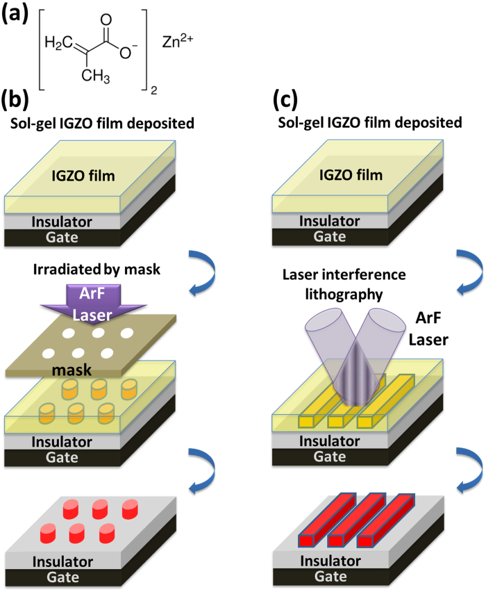
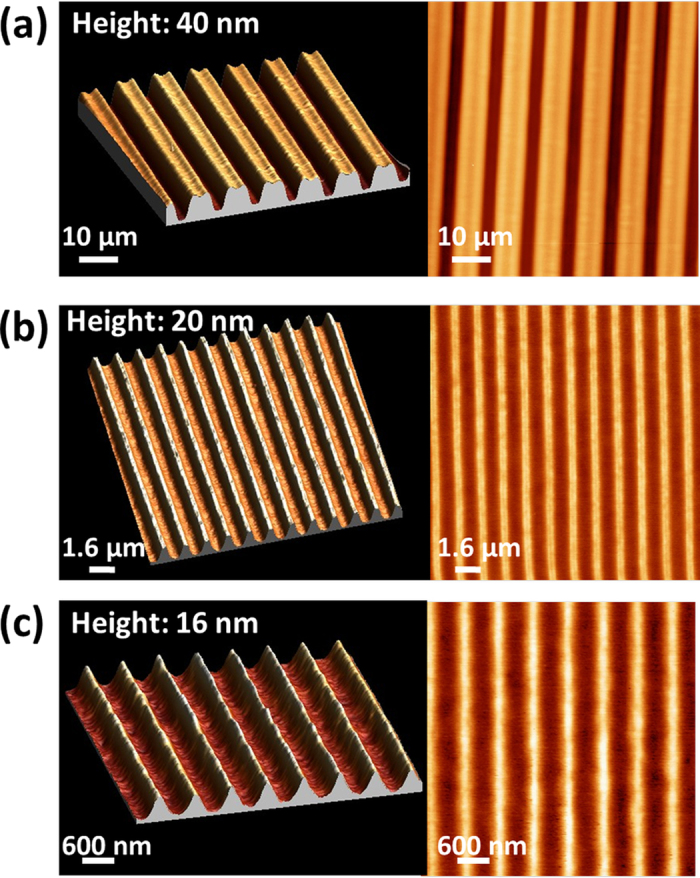
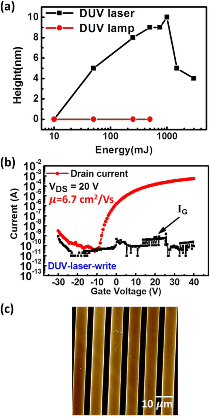
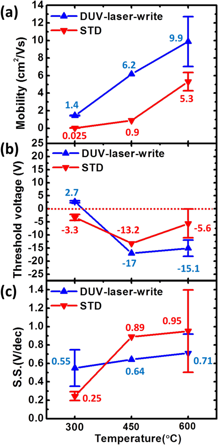
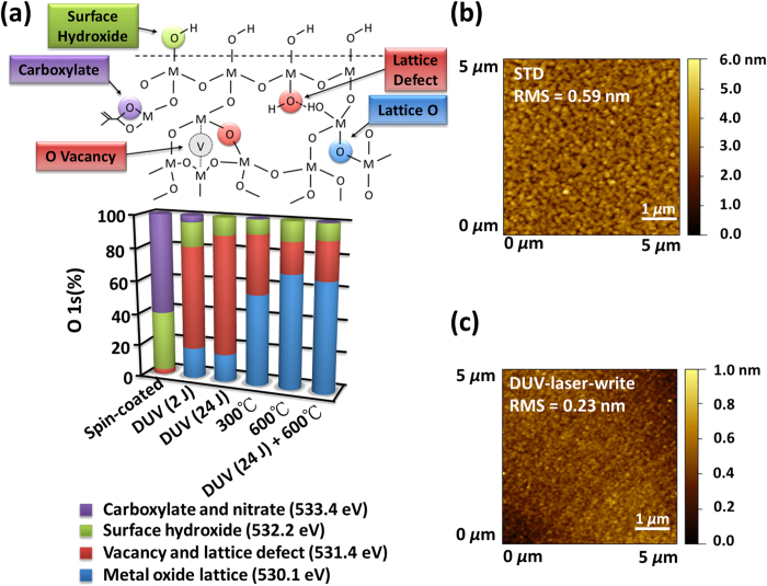
Deep-UV (DUV) laser was used to directly write indium-gallium-zinc-oxide (IGZO) precursor solution and form micro and nanoscale patterns. The directional DUV laser beam avoids the substrate heating and suppresses the diffraction effect. A IGZO precursor solution was also developed to fulfill the requirements for direct photopatterning and for achieving semi-conducting properties with thermal annealing at moderate temperature. The DUV-induced crosslinking of the starting material allows direct write of semi-conducting channels in thin-film transistors but also it improves the field-effect mobility and surface roughness. Material analysis has been carried out by XPS, FTIR, spectroscopic ellipsometry and AFM and the effect of DUV on the final material structure is discussed. The DUV irradiation step results in photolysis and a partial condensation of the inorganic network that freezes the sol-gel layer in a homogeneous distribution, lowering possibilities of thermally induced reorganization at the atomic scale. Laser irradiation allows high-resolution photopatterning and high-enough field-effect mobility, which enables the easy fabrication of oxide nanowires for applications in solar cell, display, flexible electronics, and biomedical sensors.
Figures
References
-
- Nomura K. et al. Room-temperature fabrication of transparent flexible thin-film transistors using amorphous oxide semiconductors. Nature 432, 488–492 (2004). - PubMed
-
- Kim M. G., Kanatzidis M. G., Facchetti A. & Marks T. J. Low-temperature fabrication of high-performance metal oxide thin-film electronics via combustion processing. Nature Mater. 10, 382–388 (2011). - PubMed
-
- Liu G. X. et al. High-performance fully amorphous bilayer metal-oxide thin film transistors using ultra-thin solution-processed ZrOx dielectric. Appl. Phys. Lett. 105, 113509 (2014).
-
- Chiang H. Q., Wager J. F., Hoffman R. L., Jeong J. & Keszler D. A. High mobility transparent thin-film transistors with amorphous zinc tin oxide channel layer. Appl. Phys. Lett. 86, 013503 (2005).
-
- Banger K. K. et al. Low-temperature, high-performance solution-processed metal oxide thin-film transistors formed by a ‘sol–gel on chip’ process. Nature Mater. 10, 45–50 (2011). - PubMed
Publication types
LinkOut - more resources
Full Text Sources
Other Literature Sources
Miscellaneous
