

Imaging screw dislocations at atomic resolution by aberration-corrected electron optical sectioning
- PMID: 26041257
- PMCID: PMC4468905
- DOI: 10.1038/ncomms8266
Imaging screw dislocations at atomic resolution by aberration-corrected electron optical sectioning
Abstract
Screw dislocations play an important role in materials' mechanical, electrical and optical properties. However, imaging the atomic displacements in screw dislocations remains challenging. Although advanced electron microscopy techniques have allowed atomic-scale characterization of edge dislocations from the conventional end-on view, for screw dislocations, the atoms are predominantly displaced parallel to the dislocation line, and therefore the screw displacements are parallel to the electron beam and become invisible when viewed end-on. Here we show that screw displacements can be imaged directly with the dislocation lying in a plane transverse to the electron beam by optical sectioning using annular dark field imaging in a scanning transmission electron microscope. Applying this technique to a mixed [a+c] dislocation in GaN allows direct imaging of a screw dissociation with a 1.65-nm dissociation distance, thereby demonstrating a new method for characterizing dislocation core structures.
Figures
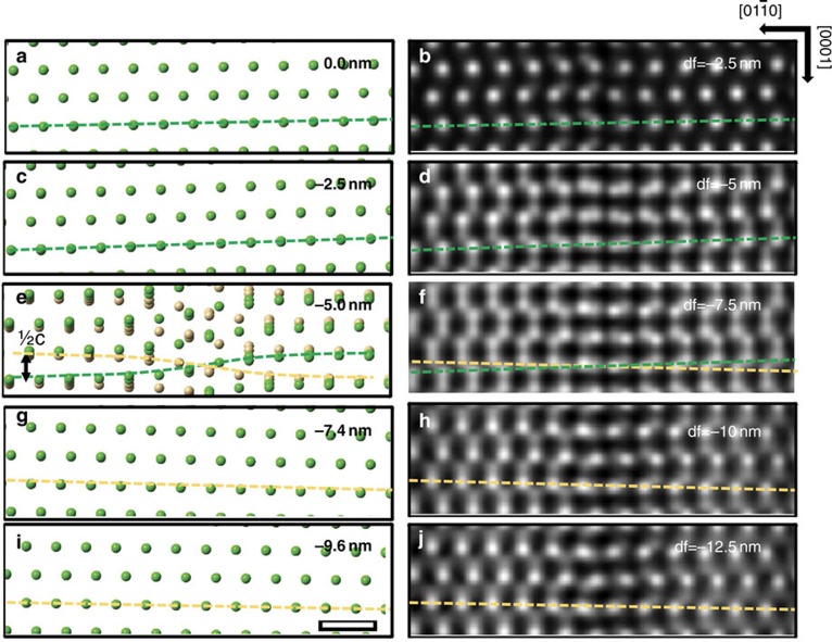
 planes at various depths in a structure model of a GaN c-type screw dislocation (left) and simulated ADF focal series images (right). The screw dislocation is along [0001] and located at a depth of −5 nm, and the single
  layers are located at a 0, c−2.5, e−5.0, g−7.4 and i−9.6 nm below the top surface, respectively. In this work depths into the crystal are given by negative values and are measured relative to the entrance surface. Similarly, negative defocus denotes under focusing so that the focal plane moves below the entrance surface into the crystal. Dashed lines show the shearing of planes due to the screw. In e, the two planes immediately above and below the dislocation line are overlaid and indicated by different colours. Owing to a channelling pre-focusing effect, each simulated focal series image on the right (b,d,f,h,j) has a focus set ∼2 nm lower in depth than the corresponding layer of model on the left. The scale bar, 0.5 nm.
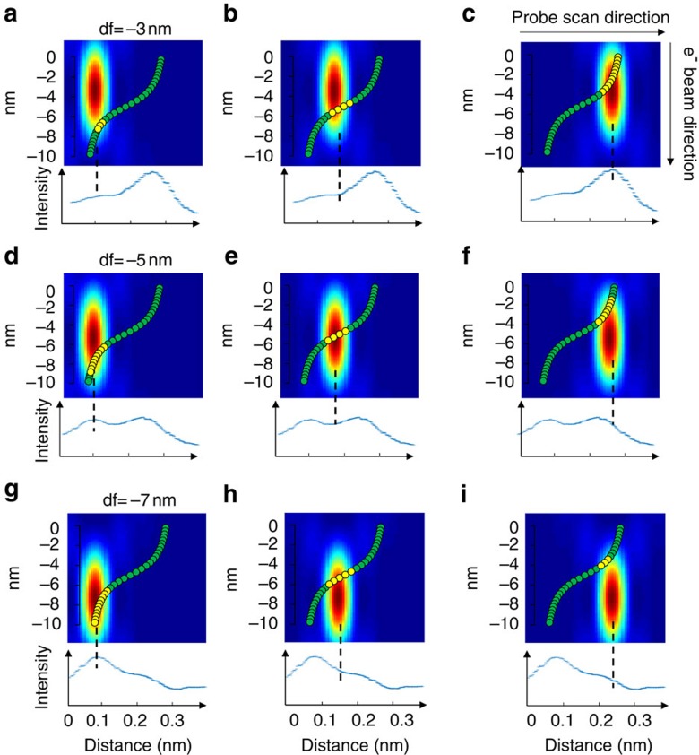

 are shown in c,d, respectively. The scale bar in the simulated image, 0.5 nm.
References
-
- Menter J. W. The direct study by electron microscopy of crystal lattices and their imperfections. Proc. R. Soc. A 236, 119–135 (1956).
-
- Hirsch P., Cockayne D., Spence J. & Whelan M. 50 years of TEM of dislocations: past, present and future. Philos. Mag. 86, 4519–4528 (2006).
-
- Xin Y. et al. Direct observation of the core structures of threading dislocations in GaN. Appl. Phys. Lett. 72, 2680–2682 (1998).
-
- Arslan I., Bleloch A., Stach E. A. & Browning N. D. Atomic and electronic structure of mixed and partial dislocations in GaN. Phys. Rev. Lett. 94, 025504 (2005). - PubMed
-
- Rhode S. K. et al. Mg doping affects dislocation core structures in GaN. Phys. Rev. Lett. 111, 25502 (2013). - PubMed
Publication types
LinkOut - more resources
Full Text Sources
Other Literature Sources
Molecular Biology Databases
