. 2015 Jul 15:6:7647.
doi: 10.1038/ncomms8647.

Intrinsically stretchable and transparent thin-film transistors based on printable silver nanowires, carbon nanotubes and an elastomeric dielectric

Affiliations

Intrinsically stretchable and transparent thin-film transistors based on printable silver nanowires, carbon nanotubes and an elastomeric dielectric

Jiajie Liang et al. Nat Commun. .

Abstract

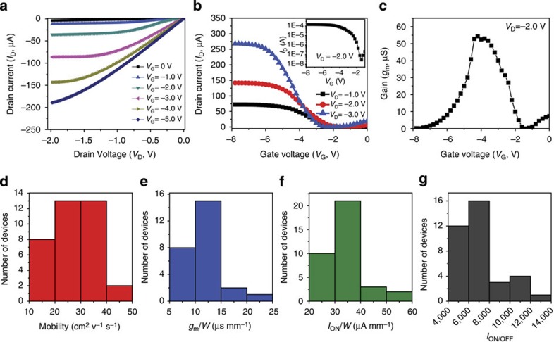
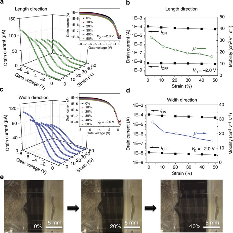
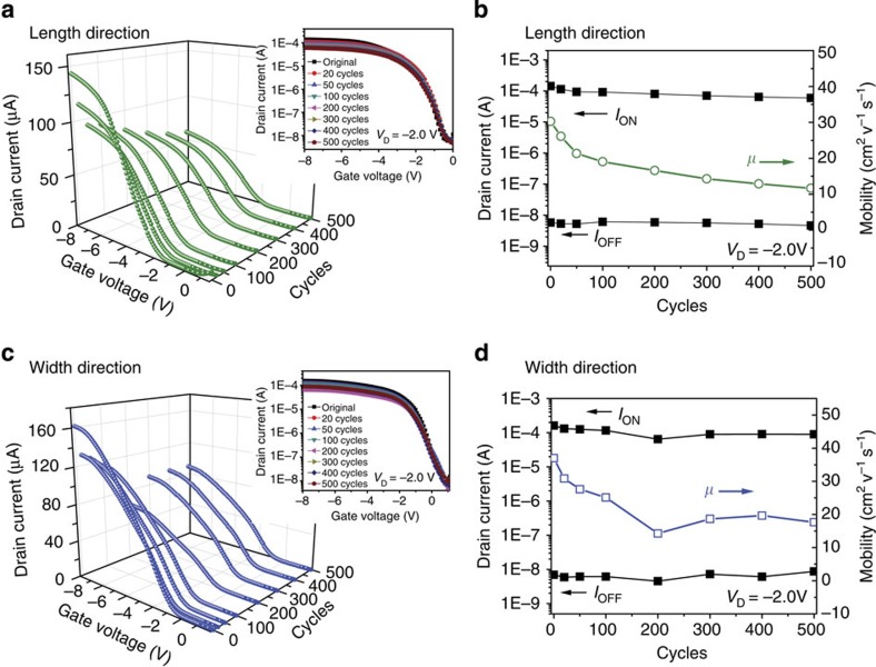
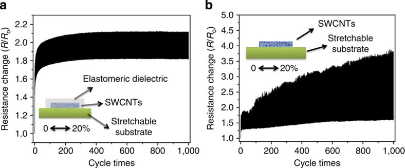
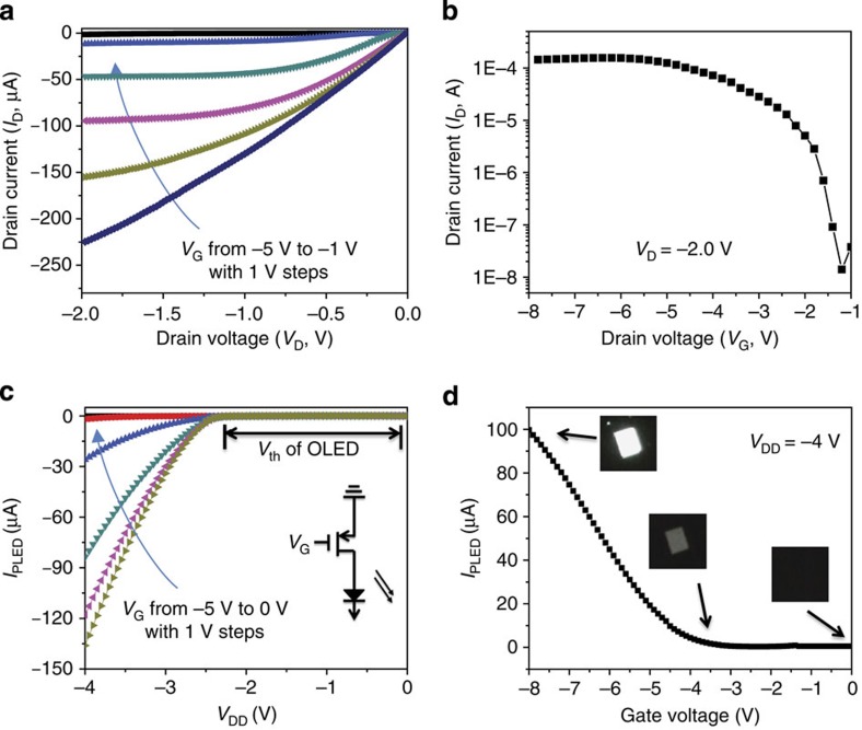
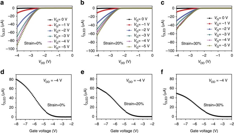
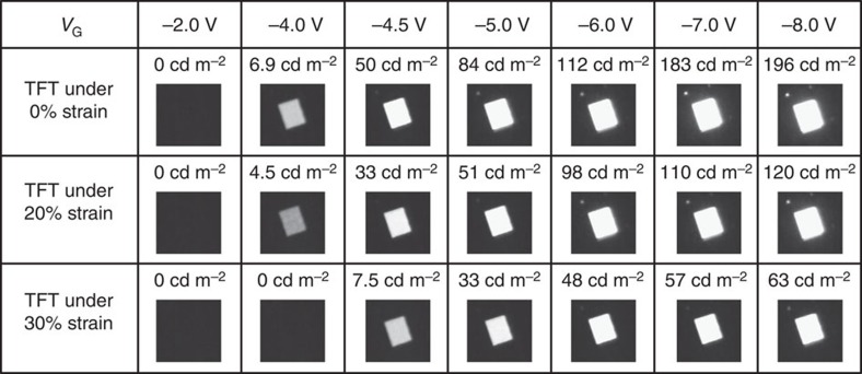
Thin-film field-effect transistor is a fundamental component behind various mordern electronics. The development of stretchable electronics poses fundamental challenges in developing new electronic materials for stretchable thin-film transistors that are mechanically compliant and solution processable. Here we report the fabrication of transparent thin-film transistors that behave like an elastomer film. The entire fabrication is carried out by solution-based techniques, and the resulting devices exhibit a mobility of ∼30 cm(2) V(-1) s(-1), on/off ratio of 10(3)-10(4), switching current >100 μA, transconductance >50 μS and relative low operating voltages. The devices can be stretched by up to 50% strain and subjected to 500 cycles of repeated stretching to 20% strain without significant loss in electrical property. The thin-film transistors are also used to drive organic light-emitting diodes. The approach and results represent an important progress toward the development of stretchable active-matrix displays.


Figures

Figure 1
Figure 1. Fabrication process and the SEM and transmittance characterizations of the stretchable TFT.
(a) Schematic illustration of the fabrication steps for a stretchable TFT. The optical microscopic image shows the AgNW-PUA composite source/drain electrodes covered with a SWCNT layer (100 μm channel length). (b) Fabrication process of AgNW-PUA composite source/drain electrodes. Inset: cross-sectional SEM image showing the SWCNTs embedded into and wrapped by the dielectric layer. (c) Optical image of a TFT array marked with a brown dash frame around the element ‘Ag'. (d) Optical transmittance of a TFT array. Inset photograph shows a folded TFT array. (e) SEM images of SWCNT network printed on AgNW-PUA composite source/drain electrodes, showing that the density can be controlled by the amount of SWCNT ink cast on the substrate.
Figure 2
Figure 2. Electrical properties of a representative stretchable TFT and statistical variation studies in the electrical properties of 36 stretchable TFTs.
(a) Output (IDVD) characteristics of a typical SWCNT-AgNW TFT (L=100 μm and W=5,000 μm) with VG from 0 to −5 V in 1 V steps. (b) Transfer (IDVG) characteristics of the same device with VD from −1.0 to −3.0 in 1.0 step. Inset, IDVG curve at VD=−2.0 V on a logarithmic scale. (c) Transconductance at VD=−2.0 V as a function of VG. (dg) Histograms of TFTs showing the statistical distribution of (d) mobility, (e) unit width normalized transconductance, (f) unit width normalized ION and (g) the ION/OFF.
Figure 3
Figure 3. The device performance changes with tensile strain.
(a) Typical transfer characteristics (VD=−2.0 V) of a TFT device under specific tensile strain applied along the channel length direction. The insets show log-scale characteristics. (b) ION, IOFF and mobility as a function of applied strain along the channel length direction. (c) Typical transfer characteristics (VD=−2.0 V) of a device under specific tensile strain applied along the channel width direction. The insets show log-scale characteristics. (d) ION, IOFF and mobility as a function of applied strain along the channel width direction. (e) Magnified photographs of a device at specified strains applied along the channel length direction. Scale bar=5 mm.
Figure 4
Figure 4. Fatigue testing when stretching and releasing 500 times.
(a) Typical transfer characteristics (VD=−2.0 V) of a TFT device after specified cycles of 20% tensile strain applied along the channel length direction. The insets show log-scale characteristics. (b) Plots of ION and IOFF at 0% strain during 500 cycles of continuous stretching–relaxing between 0 and 20% strains along the channel length direction. (c) Typical transfer characteristics (VD=−2.0 V) of a device after specified cycles of 20% tensile strain applied along the channel width direction. The insets show log-scale characteristics. (d) Plots of ION and IOFF at 0% strain during 500 cycles of continuous stretching–relaxing between 0 and 20% strains along the channel width direction.
Figure 5
Figure 5. Mechanical compliance of SWCNT network on PUA substrate.
Normalized transient resistance of SWCNT coated on PUA substrate with (a) and without (b) the elastomeric dielectric overcoat during 1,000 cycles of tensile stretching and releasing between 0 and 20% strains.
Figure 6
Figure 6. OLED control circuit driven by stretchable TFT.
Stretchable SWCNT-AgNW TFT to control OLED devices. (a) Output (IDVD) characteristics of the TFT device used to control an OLED with different gate voltage. (b) Transfer (IDVG) characteristics of the TFT under VD=−2.0 V. (c) IOLEDVDD characteristics of the OLED control circuit with different VG. Inset: schematic diagram of the OLED control circuit. (d) Plot of the IOLED over VG with VDD=−4.0 V. The inset photographs show the OLED brightness at specific VG.
Figure 7
Figure 7. Characterization of OLED control circuit with stretchable TFT under different strains.
Output (IOLEDVDD) characteristics of the OLED controlled by a stretchable SWCNT-AgNW TFT. The TFT is stretched along channel length direction by (a) 0%, (b) 20% and (c) 30% strains. The VG is varied from 0 to −5.0 V in 1 V increments. Transfer (IOLEDVG) characteristics at VDD=−4.0 V for the TFT device used to control the OLED under 0% (d), 20% (e) and 30% (f) strains.
Figure 8
Figure 8. Luminance of an OLED driven by stretchable TFT under different inputs.
Luminance was investigated for the TFT under strains (along channel length direction) of 0, 20 and 30%, respectively. VDD is −4.0 V.

References

    1. White M. S. et al.. Ultrathin, highly flexible and stretchable PLEDs. Nat. Photonics 7, 811–816 (2013).
    1. Xu S. et al.. Soft microfluidic assemblies of sensors, circuits, and radios for the skin. Science 344, 70–74 (2014). - PubMed
    1. Savagatrup S., Printz A. D., O'Connor T. F., Zaretski A. V. & Lipomi D. J. Molecularly stretchable electronics. Chem. Mater. 26, 3028–3041 (2014).
    1. Kim R. H. et al.. Waterproof AlInGaP optoelectronics on stretchable substrates with applications in biomedicine and robotics. Nat. Mater. 9, 929–937 (2010). - PubMed
    1. Filiatrault H. L., Porteous G. C., Stephen R., Davidson G. J. E. & Breen T. Stretchable light-emitting electrochemical cells using an elastomeric emmissive material. Adv. Mater. 24, 2673–2678 (2012). - PubMed

Publication types