. 2015 Jul 20:5:12285.
doi: 10.1038/srep12285.

Electronic, Dielectric, and Plasmonic Properties of Two-Dimensional Electride Materials X2N (X=Ca, Sr): A First-Principles Study

Affiliations

Electronic, Dielectric, and Plasmonic Properties of Two-Dimensional Electride Materials X2N (X=Ca, Sr): A First-Principles Study

Shan Guan et al. Sci Rep. .

Abstract

Based on first-principles calculations, we systematically study the electronic, dielectric, and plasmonic properties of two-dimensional (2D) electride materials X2N (X=Ca, Sr). We show that both Ca2N and Sr2N are stable down to monolayer thickness. For thicknesses larger than 1-monolayer (1-ML), there are 2D anionic electron layers confined in the regions between the [X2N](+) layers. These electron layers are strongly trapped and have weak coupling between each other. As a result, for the thickness dependence of many properties such as the surface energy, work function, and dielectric function, the most dramatic change occurs when going from 1-ML to 2-ML. For both bulk and few-layer Ca2N and Sr2N, the in-plane and out-of-plane real components of their dielectric functions have different signs in an extended frequency range covering the near infrared, indicating their potential applications as indefinite media. We find that bulk Ca2N and Sr2N could support surface plasmon modes in the near infrared range. Moreover, tightly-bounded plasmon modes could exist in their few-layer structures. These modes have significantly shorter wavelengths (few tens of nanometers) compared with that of conventional noble metal materials, suggesting their great potential for plasmonic devices with much smaller dimensions.


Conflict of interest statement

The authors declare no competing financial interests.

Figures

Figure 1
Figure 1
a Top and b side view of crystal structure of 3-ML X2N (X = Ca, Sr). It consists of three (X-N-X) unit layers with ABC-stacking. The symbols L1, L2, and G12 refer to the thicknesses of outermost layer, the next outermost layer, and the interlayer gap between L1 and L2, respectively, as explained in the caption of Tabel 1.
Figure 2
Figure 2. Phonon dispersions.
a, Phonon dispersion of 1-ML Ca2N. b, Phonon dispersion of 1-ML Sr2N.
Figure 3
Figure 3. Surface energies for few-layer Ca2N and Sr2N as a function of thickness d from 1-ML to 5-ML.
Figure 4
Figure 4. Electronic band structures of few-layer Ca2N and Sr2N.
a-c, Band structure of Ca2N with a 1-ML, b 2-ML, and c 3-ML thickness. d-f, Band structure of Sr2N with d 1-ML, e 2-ML, and f 3-ML thickness. Fermi energy is set at zero. The two green colored bands are mainly from the 2D electron layers confined to the surface. The red colored bands (for films thicker than 1-ML) are mainly from the 2D electron layers confined in the interlayer regions. The red shaded rectangles in a and d indicate the regions contributing to the peaks ~0.3 eV in interband Imε(ω) for 1-ML Ca2N and Sr2N.
Figure 5
Figure 5. Electron density distribution in 2-ML Ca2N.
a, Partial electron density isosurfaces (with value of 0.0003/Bohr3) for states in the energy range |E − Ef| < 0.05 eV shown for a conventional unit cell. b-d, Band-decomposed electron density isosurfaces (with value of 0.003/Bohr3) for the three (colored) bands which cross Fermi level as shown in Fig. 4(b). b is for the upper green band, c is for the lower green band, and d is for the red band.
Figure 6
Figure 6. Work functions for few-layer Ca2N and Sr2N as a function of thickness d from 1-ML to 5-ML.
Figure 7
Figure 7
Partial density of states for the energy range |E − Ef| < 0.05 eV averaged over the ab plane for a 2-ML Ca2N and b 2-ML Sr2N. In each figure, the blue curve and the red curve are for the distributions before and after one valence electron is removed, respectively. The green shaded regions indicate the locations of the [Ca2N]+ or [Sr2N]+ layers.
Figure 8
Figure 8
Anisotropic dielectric functions for bulk X2N: a for Ca2N and b for Sr2N. The real and imaginary parts of in-plane component εxx and out-of-plane component εzz are plotted using different colors. The blue shaded region in each figure indicates the frequency range in which Reεxx and Reεzz have different signs.
Figure 9
Figure 9
a, In-plane plasma frequency ωp,xx for Ca2N and Sr2N thin films as a function of thickness d from 1-ML to 5-ML. b, electron density of states (DOS) of Ca2N and Sr2N at Fermi energy as a function of film thickness. In each figure, the dashed lines indicate the corresponding values for the bulk.
Figure 10
Figure 10
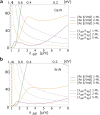
The interband contribution to Imεxx(ω) for a Ca2N and b Sr2N thin film structures from 1-ML to 5-ML. Results for different thicknesses are plotted using different colors.
Figure 11
Figure 11
Dispersion relation of surface plasmon modes for an interface between a dielectric medium with εd = 2.25 and bulk X2N (X = Ca, Sr). The light line in the dielectric medium is also shown in grey color.
Figure 12
Figure 12
Dispersion characteristics of surface plasmon modes for Ca2N few-layers in a dielectric medium with εd = 2.25. a and b are for the antisymmetric mode (L+ mode). c and d are for the symmetric mode (L− mode). a and c show the real part of the wave number component. b and d show the imaginary part of the wave number component.
Figure 13
Figure 13
Characteristics Reβ/Imβ and λairsp for the symmetric surface plasmon modes in few-layer a Ca2N and b Sr2N, plotted as functions of the wavelength in air λair. λsp is the surface plasmon wavelength. The dielectric medium is with εd = 2.25.

References

    1. Dye J. L. Electrons as Anions. Science 301, 607–608 (2003). - PubMed
    1. Dye J. L. Electrides: early examples of quantum confinement. Acc.Chem.Res. 42, 1564–1572 (2009). - PubMed
    1. Ellaboudy A., Dye J. L. & Smith P. B. Cesium 18-Crown-6 Compounds. A Crystalline Ceside and a Crystalline Electride. J. Am. Chem. Soc. 105, 6490–6491 (1983).
    1. Huang R. H., Faber M. K., Moeggenborg K. J., Ward D. L. & Dye J. L. Structure of K+ (cryptand[2.2.2J) electride and evidence for trapped electron pairs. Nature 331, 599–601 (1988).
    1. Dye J. L. Electrides: Ionic Salts with Electrons as the Anions. Science 247, 663–668 (1990). - PubMed

Publication types