

Performing elemental microanalysis with high accuracy and high precision by scanning electron microscopy/silicon drift detector energy-dispersive X-ray spectrometry (SEM/SDD-EDS)
- PMID: 26346887
- PMCID: PMC4555346
- DOI: 10.1007/s10853-014-8685-2
Performing elemental microanalysis with high accuracy and high precision by scanning electron microscopy/silicon drift detector energy-dispersive X-ray spectrometry (SEM/SDD-EDS)
Abstract
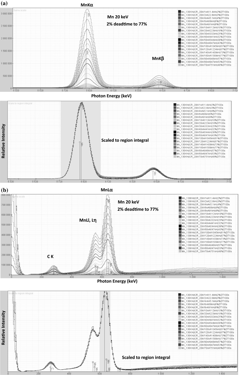
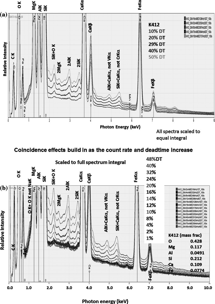
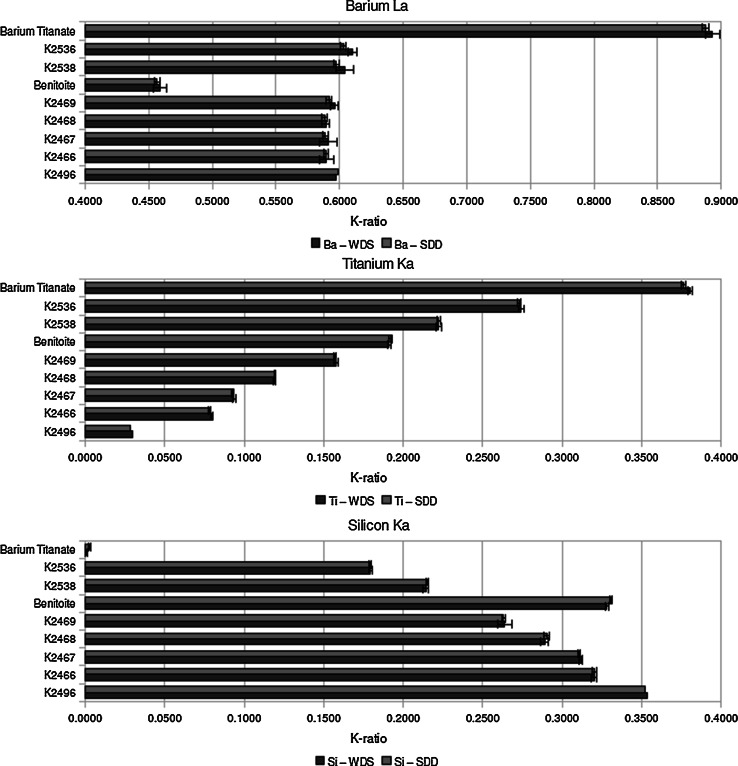
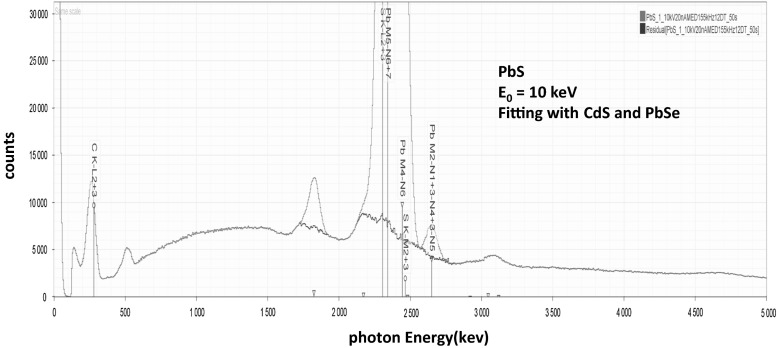
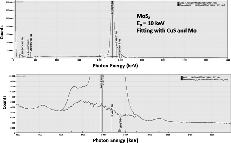
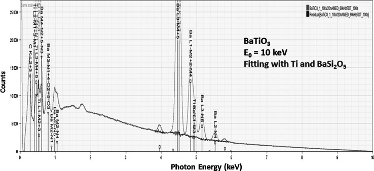
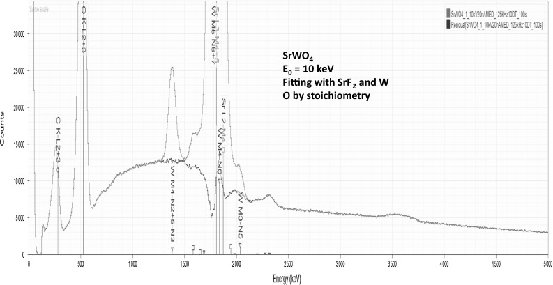
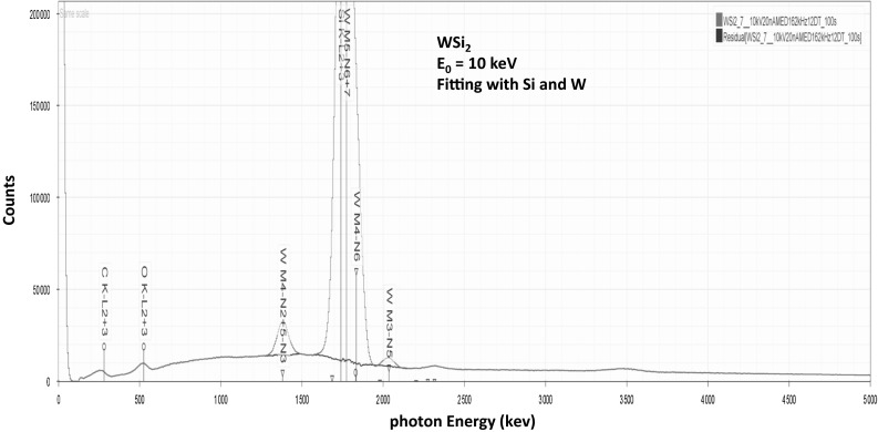
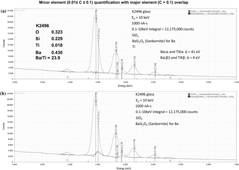
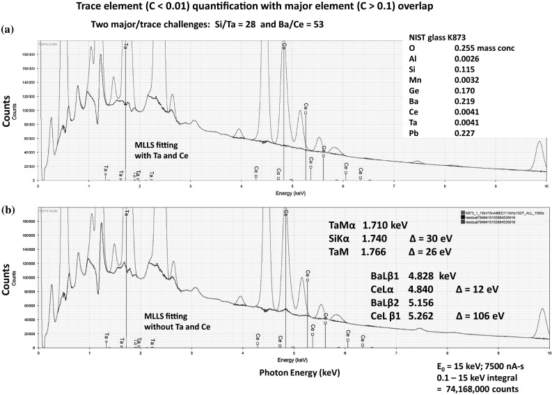
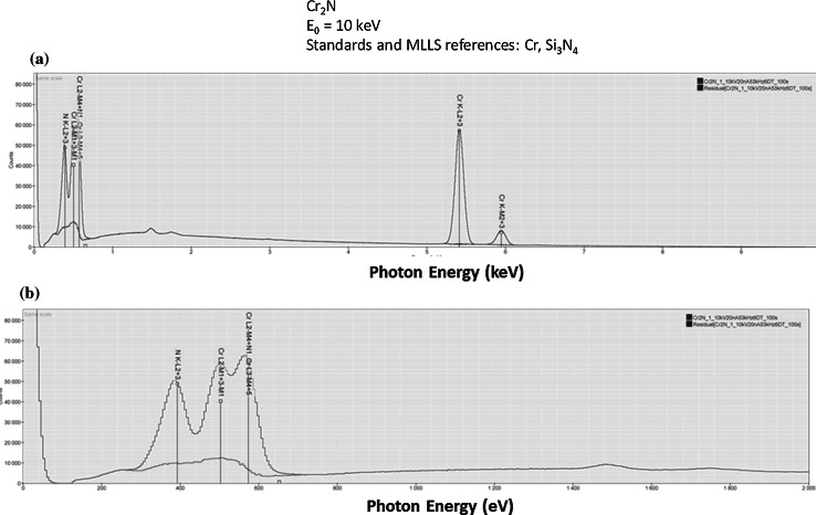
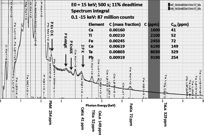
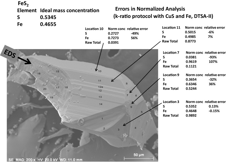
Electron-excited X-ray microanalysis performed in the scanning electron microscope with energy-dispersive X-ray spectrometry (EDS) is a core technique for characterization of the microstructure of materials. The recent advances in EDS performance with the silicon drift detector (SDD) enable accuracy and precision equivalent to that of the high spectral resolution wavelength-dispersive spectrometer employed on the electron probe microanalyzer platform. SDD-EDS throughput, resolution, and stability provide practical operating conditions for measurement of high-count spectra that form the basis for peak fitting procedures that recover the characteristic peak intensities even for elemental combination where severe peak overlaps occur, such PbS, MoS2, BaTiO3, SrWO4, and WSi2. Accurate analyses are also demonstrated for interferences involving large concentration ratios: a major constituent on a minor constituent (Ba at 0.4299 mass fraction on Ti at 0.0180) and a major constituent on a trace constituent (Ba at 0.2194 on Ce at 0.00407; Si at 0.1145 on Ta at 0.0041). Accurate analyses of low atomic number elements, C, N, O, and F, are demonstrated. Measurement of trace constituents with limits of detection below 0.001 mass fraction (1000 ppm) is possible within a practical measurement time of 500 s.
Figures
Similar articles
-
Is scanning electron microscopy/energy dispersive X-ray spectrometry (SEM/EDS) quantitative?Scanning. 2013 May-Jun;35(3):141-68. doi: 10.1002/sca.21041. Epub 2012 Aug 9. Scanning. 2013. PMID: 22886950
-
Measurement of Trace Constituents by Electron-Excited X-Ray Microanalysis with Energy-Dispersive Spectrometry.Microsc Microanal. 2016 Jun;22(3):520-35. doi: 10.1017/S1431927616000738. Microsc Microanal. 2016. PMID: 27329308
-
Quantitative Electron-Excited X-Ray Microanalysis of Borides, Carbides, Nitrides, Oxides, and Fluorides with Scanning Electron Microscopy/Silicon Drift Detector Energy-Dispersive Spectrometry (SEM/SDD-EDS) and NIST DTSA-II.Microsc Microanal. 2015 Oct;21(5):1327-40. doi: 10.1017/S1431927615014993. Epub 2015 Sep 14. Microsc Microanal. 2015. PMID: 26365439
-
Elemental analysis of occupational and environmental lung diseases by electron probe microanalyzer with wavelength dispersive spectrometer.Respir Investig. 2014 Jan;52(1):5-13. doi: 10.1016/j.resinv.2013.05.002. Epub 2013 Jul 5. Respir Investig. 2014. PMID: 24388365 Review.
-
Calcium measurements with electron probe X-ray and electron energy loss analysis.Environ Health Perspect. 1990 Mar;84:57-73. doi: 10.1289/ehp.908457. Environ Health Perspect. 1990. PMID: 2190819 Free PMC article. Review.
Cited by
-
Nonvolatile Isomorphic Valence Transition in SmTe Films.ACS Nano. 2024 Jan 30;18(4):2972-2981. doi: 10.1021/acsnano.3c07960. Epub 2024 Jan 16. ACS Nano. 2024. PMID: 38228321 Free PMC article.
-
UMAOH Calcium Phosphate Coatings Designed for Drug Delivery: Vancomycin, 5-Fluorouracil, Interferon α-2b Case.Materials (Basel). 2022 Jul 1;15(13):4643. doi: 10.3390/ma15134643. Materials (Basel). 2022. PMID: 35806777 Free PMC article.
-
Structural Analysis of Si(OEt)4 Deposits on Au(111)/SiO2 Substrates at the Nanometer Scale Using Focused Electron Beam-Induced Deposition.ACS Omega. 2023 Jun 28;8(27):24233-24246. doi: 10.1021/acsomega.3c00793. eCollection 2023 Jul 11. ACS Omega. 2023. PMID: 37457449 Free PMC article.
-
Certification of New Standard Reference Material 2806b Medium Test Dust in Hydraulic Fluid.J Res Natl Inst Stand Technol. 2016 Dec 19;121:476-497. doi: 10.6028/jres.121.025. eCollection 2016. J Res Natl Inst Stand Technol. 2016. PMID: 34434636 Free PMC article.
-
Metagenomic Insights into Pollutants in Biorefinery and Dairy Wastewater: rDNA Dominance and Electricity Generation in Double Chamber Microbial Fuel Cells.Bioengineering (Basel). 2025 Jan 19;12(1):88. doi: 10.3390/bioengineering12010088. Bioengineering (Basel). 2025. PMID: 39851362 Free PMC article.
References
-
- Castaing R (1951) Application of electron probes to metallographic analysis. Ph.D. Dissertation, University of Paris
-
- Goldstein J, Newbury D, Joy D, Lyman C, Echlin P, Lifshin E, Sawyer L, Michael J. Scanning electron microscopy and X-ray microanalysis. 3. New York: Springer; 2003.
-
- Heinrich K. Electron beam X-ray microanalysis. New York: Van Nostrand Reinhold; 1981. pp. 99–140.
-
- Yakowitz H (1968) Evaluation of specimen preparation and the use of standards in electron probe microanalysis. In: Fifty years of progress in metallographic techniques, ASTM-special technical publication 430. American Society of Testing and Materials, Philadelphia 430, pp 383–408
-
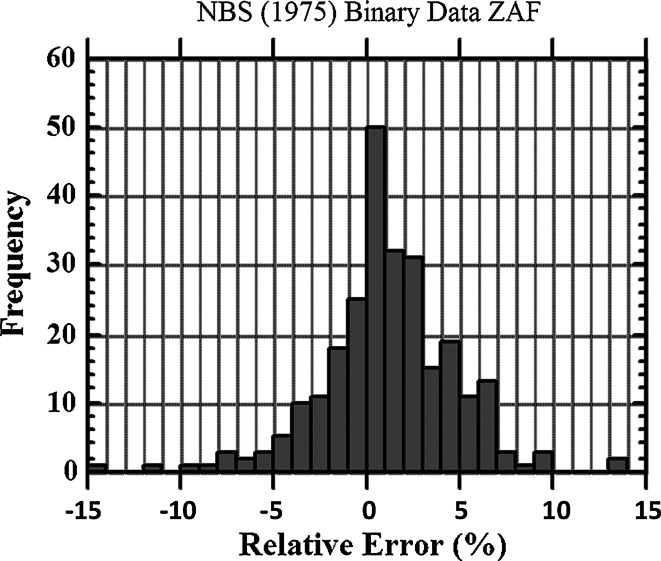
- Yakowitz H (1975) Methods of quantitative analysis. In: Goldstein JI, Yakowitz H, Newbury DE, Lifshin E, Colby JW, Coleman JR (eds.) Practical scanning electron microscopy. Plenum, New York, p 338 (error histogram derived from Heinrich K, Yakowitz H, Vieth D (1972) Proceedings of 7th conference electron probe analysis, Microanalysis Society)
Publication types
LinkOut - more resources
Full Text Sources
Other Literature Sources