. 2015 Sep 24:6:8195.
doi: 10.1038/ncomms9195.

High charge mobility in two-dimensional percolative networks of PbSe quantum dots connected by atomic bonds

Affiliations

High charge mobility in two-dimensional percolative networks of PbSe quantum dots connected by atomic bonds

Wiel H Evers et al. Nat Commun. .

Abstract

Two-dimensional networks of quantum dots connected by atomic bonds have an electronic structure that is distinct from that of arrays of quantum dots coupled by ligand molecules. We prepared atomically coherent two-dimensional percolative networks of PbSe quantum dots connected via atomic bonds. Here, we show that photoexcitation leads to generation of free charges that eventually decay via trapping. The charge mobility probed with an AC electric field increases with frequency from 150 ± 15 cm(2) V(-1) s(-1) at 0.2 terahertz to 260 ± 15 cm(2) V(-1) s(-1) at 0.6 terahertz. Gated four-probe measurements yield a DC electron mobility of 13 ± 2 cm(2) V(-1) s(-1). The terahertz mobilities are much higher than for arrays of quantum dots coupled via surface ligands and are similar to the highest DC mobilities reported for PbSe nanowires. The terahertz mobility increases only slightly with temperature in the range of 15-290 K. The extent of straight segments in the two-dimensional percolative networks limits the mobility, rather than charge scattering by phonons.


Figures

Figure 1
Figure 1. Optical absorption spectra and structure of 2D PbSe networks.
(a) Optical absorption spectra of 2D PbSe networks and PbSe QDs in dispersion. (b) TEM image of a network of relatively weakly coupled QDs obtained by heating at 30 °C (15 min). (c) 2D percolative network of fused QDs obtained after subsequent heating in two steps, first at 50 °C (15 min) and subsequently at 80 °C (15 min). The presence of diffraction spots in the electrodiffractogram in the upper right corner implies that crystal planes in different QDs have the same orientation. The scale bars for the TEM images, TEM insets and electrodiffractogram represent 40 nm, 5 nm and 0.25 nm, respectively.
Figure 2
Figure 2. Optical bleach and THz conductivity after photoexcitation.
(a) Long timescale optical bleach (left axis) and real component of the THz conductivity (right axis) normalized at a time of 10 ps and offset vertically for clarity. The dashed curves are fits of a stretched-exponential. (b) Short timescale product of the sum of the quantum yields of electrons and holes, ϕe(t)+ϕh(t), and the cross section for bleach, σ (see Methods). (c) Short timescale sum of the quantum yield of electrons and holes, weighted by their real or imaginary mobility, μ, averaged over the frequency range 0.3–0.5 THz (see Methods).
Figure 3
Figure 3. Frequency dependence of the charge mobility.
Real (upper panel) and imaginary (lower panel) components of the charge mobility at 15 and 290 K, averaged over pump–probe time delays in the interval 8–12 ps. The uncertainty in the mobility data is determined by fluctuations in the pump laser fluence. The increase of the magnitude of the real and imaginary mobility is typical for charge motion that is hindered by scattering at barriers to transport. The solid curves are fits of the Drude-Smith model to the experimental mobility data.
Figure 4
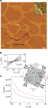
Figure 4. DC transport characteristics.
(a) SEM image of a network deposited on a 50-nm-thick SiO2 layer with the dark alveoli and the bright stripes corresponding to the bottom layer and bilayer, respectively. The scale bar in the lower-right corner represents 200 nm. Inset: high-resolution SEM image obtained at the boundary between a bottom layer and the bilayer. The scale bar in the lower-right corner represents 20 nm. (b) Two-terminal current versus voltage at different gate voltages obtained on the bottom layer. (c) Four-terminal resistance of a single percolative network measured with a square arrangement of the STM tips at a separation of 500 nm. The direction of the current and the potential drop with respect to the network rows are indicated in the SEM image in the inset.

References

    1. Talapin D. V., Lee J.-S., Kovalenko M. V. & Shevchenko E. V. Prospects of colloidal nanocrystals for electronic and optoelectronic applications. Chem. Rev. 110, 389–458 (2010). - PubMed
    1. Krahne R. et al.. Physical properties of elongated inorganic nanoparticles. Phys. Rep. 501, 75–221 (2011).
    1. Bouet C. et al.. Flat colloidal semiconductor nanoplatelets. Chem. Mater. 25, 1262–1271 (2013).
    1. Schliehe C. et al.. Ultrathin PbS sheets by two-dimensional oriented attachment. Science 329, 550–553 (2010). - PubMed
    1. Evers W. H. et al.. Low-dimensional semiconductor superlattices formed by geometric control over nanocrystal attachment. Nano Lett. 13, 2317–2323 (2013). - PubMed

Publication types