. 2015 Oct 9:6:8475.
doi: 10.1038/ncomms9475.

Wafer-scale growth of VO2 thin films using a combinatorial approach

Affiliations

Wafer-scale growth of VO2 thin films using a combinatorial approach

Hai-Tian Zhang et al. Nat Commun. .

Abstract

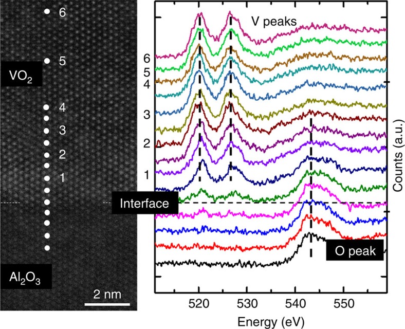
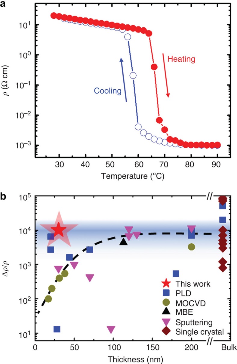
Transition metal oxides offer functional properties beyond conventional semiconductors. Bridging the gap between the fundamental research frontier in oxide electronics and their realization in commercial devices demands a wafer-scale growth approach for high-quality transition metal oxide thin films. Such a method requires excellent control over the transition metal valence state to avoid performance deterioration, which has been proved challenging. Here we present a scalable growth approach that enables a precise valence state control. By creating an oxygen activity gradient across the wafer, a continuous valence state library is established to directly identify the optimal growth condition. Single-crystalline VO2 thin films have been grown on wafer scale, exhibiting more than four orders of magnitude change in resistivity across the metal-to-insulator transition. It is demonstrated that 'electronic grade' transition metal oxide films can be realized on a large scale using a combinatorial growth approach, which can be extended to other multivalent oxide systems.


Figures

Figure 1
Figure 1. Combinatorial growth method.
(a) Schematic of V-effusion cell, VTIP gas injector and a 3-inch wafer arrangement to create a gradient of VTIP:V flux ratios along the equatorial line across the wafer. (b) Resistivity at 30 (insulating state) and 80 °C (metallic state) measured from nine devices of VO2 on r-Al2O3 located at different positions on the equatorial line. (c) Schematic of V-effusion cell, VTIP gas injector and 1 × 1 cm substrates arrangement for the growth of VO2 films with varying equivalent VTIP fluxes from sample to sample. (d) Resistivity at 30 (insulating state) and 80 °C (metallic state) of five 1 × 1 cm samples grown using the set-up in c. (e) Calculated equivalent VTIP flux distribution across a 3-inch wafer with 4.5 × 10⁻⁷ torr VTIP ion gauge pressure. For size comparison, the green square at the center represents a 1 × 1-cm sample. The colour key provided in e also applies to b,d and f. (f) Superposition of the resistivity data shown in b and d. The position axis in b was converted to equivalent VTIP flux using the flux profile calculated from equation (1) that is shown in e.
Figure 2
Figure 2. Characterization of VO2 films grown on a 3-inch r plane sapphire substrate.
(a) Comparison of substrate sizes used for the VO2 thin-film growth. (b) Streaky RHEED pattern of VO2 films observed along [100] azimuth after growth. (c) Wide range 2θω X-ray diffraction scans of VO2 grown on a r planeAl2O3 substrate. (d) AFM scan of the film surface morphology and a line scan along AB.
Figure 3
Figure 3. Wafer-scale metrology of VO2 grown on a 3-inch r plane sapphire substrate.
The squares in the schematic on the left represent the probing locations on the wafer. (a) Film thickness uniformity extracted from spectroscopic ellipsometry measurements. (b) Map of the out-of-plane lattice parameter determined from X-ray diffraction scans.
Figure 4
Figure 4. Wafer-scale mapping of MIT properties of 3-inch VO2.
(a) Schematic with squares showing the probing locations on the wafer. (b) Definition of the MIT properties: resistivity ratio (Δρ/ρ), transition point (Th and Tc), transition sharpness (ΔTh and ΔTc) and transition width (ΔH). The subscripts h and c indicate the cooling and heating cycle, respectively. Closed red and open blue circles represent heating and cooling cycles, respectively. (c) Map of VO2 resistivity ratio Δρ/ρ=(ρ30 °Cρ80 °C)/ρ80 °C obtained from four-point–probe measurements of resistivity ρ30 °C at 30 °C (VO2 insulating state) and ρ80 °C at 80 °C (VO2 metallic state). Wafer-scale mapping of MIT properties defined in b across the 3-inch VO2 film: (d) ΔH, (e) Th, (f) Tc, (g) ΔTh, (h) ΔTc.
Figure 5
Figure 5. STEM and EELS characterization.
High-angle annular dark-field scanning transmission electron microscopy (HAADF-STEM) image of the VO2/Al2O3 interface. Since Vanadium has a higher atomic number compared with Aluminum (23 versus 13), the film can be distinguished compared with the substrate by the higher intensity vanadium atoms. Electron energy loss spectroscopy (EELS) to determine the vanadium valence across the interface is shown on the right. EELS spectra were taken at the position indicated in the STEM image. The EELS data were collected from a beam spot size with ∼1-Å diameter.
Figure 6
Figure 6. Benchmark of VO2 thin films.
(a) Temperature-dependent resistivity of VO2 films grown under optimized condition on a 3-inch r plane Al2O3. Measurement was taken at the wafer center. (b) Benchmark of resistivity ratios Δρ/ρ=(ρ50 °Cρ80 °C)/ρ80 °C for VO2 across the metal-to-insulator transition. Note that the low temperature resistivity was taken at 50 °C. For a direct comparison, all films were grown on Al2O3 substrates above the critical films thickness. The blue-shaded area indicates the highest values reported for VO2 films on sapphire and typical values obtained in bulk single crystals. A dotted line was added as guide to the eye. Note the two PLD samples with resistivity ratios higher than Δρ/ρ=103 at film thicknesses <25 nm, from ref. . A thickness much >200 nm was estimated for the VO2 films grown by PLD in ref. and the data were added as ‘bulk' value. Data for bulk VO2 were taken from refs , , , , , , . Properties of VO2 films on Al2O3 substrate grown by PLD were taken from refs , , , , , , , , MOCVD from refs , , MBE from ref. and sputtering from refs , , , , , , .

References

    1. Jany R. et al. Monolithically integrated circuits from functional oxides. Adv. Mater. Interfaces 1, 1–7 (2014).
    1. Mathews S., Ramesh R., Venkatesan T. & Benedetto J. Ferroelectric field effect transistor based on epitaxial perovskite heterostructures. Science 276, 238–240 (1997). - PubMed
    1. Takagi H. & Hwang H. Y. An emergent change of phase for electronics. Science 327, 1601–1602 (2010). - PubMed
    1. Assmann E. et al. Oxide heterostructures for efficient solar cells. Phys. Rev. Lett. 110, 078701 (2013). - PubMed
    1. Katzke H., Tolédano P. & Depmeier W. Theory of morphotropic transformations in vanadium oxides. Phys. Rev. B 68, 024109 (2003).

Publication types