

Quantifying the barrier lowering of ZnO Schottky nanodevices under UV light
- PMID: 26456370
- PMCID: PMC4601028
- DOI: 10.1038/srep15123
Quantifying the barrier lowering of ZnO Schottky nanodevices under UV light
Abstract
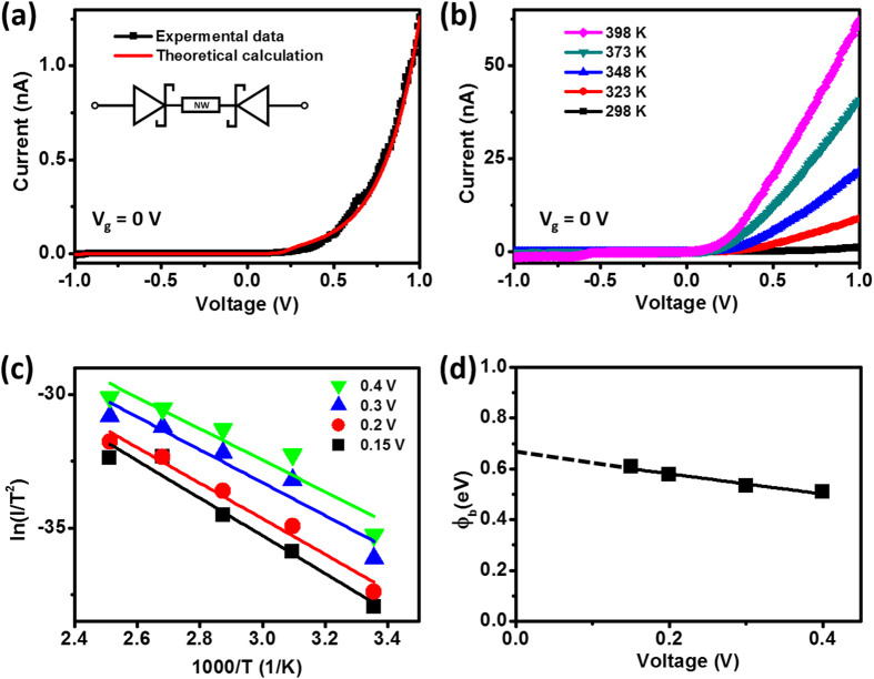
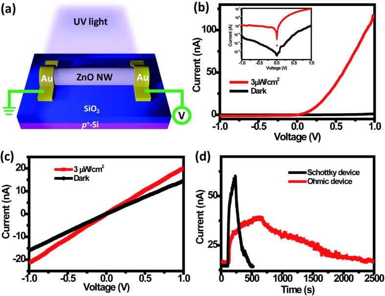
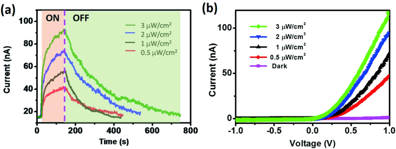
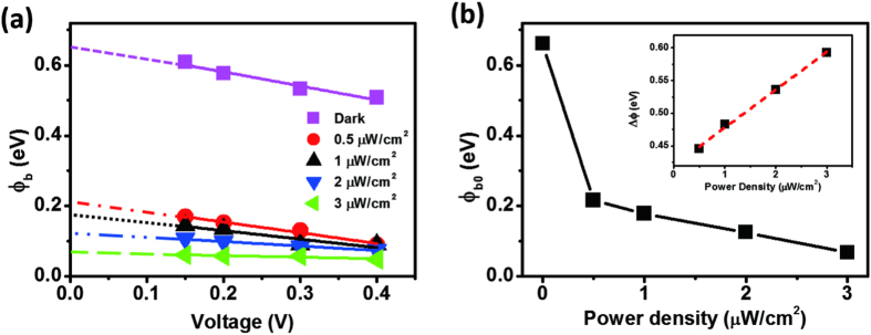
In this study we measured the degrees to which the Schottky barrier heights (SBHs) are lowered in ZnO nanowire (NW) devices under illumination with UV light. We measured the I-V characteristics of ZnO nanowire devices to confirm that ZnO is an n-type semiconductor and that the on/off ratio is approximately 10(4). From temperature-dependent I-V measurements we obtained a SBH of 0.661 eV for a ZnO NW Schottky device in the dark. The photosensitivity of Schottky devices under UV illumination at a power density of 3 μW/cm(2) was 9186%. Variations in the SBH account for the superior characteristics of n-type Schottky devices under illumination with UV light. The SBH variations were due to the coupled mechanism of adsorption and desorption of O2 and the increase in the carrier density. Furthermore, through temperature-dependent I-V measurements, we determined the SBHs in the dark and under illumination with UV light at power densities of 0.5, 1, 2, and 3 μW/cm(2) to be 0.661, 0.216, 0.178, 0.125, and 0.068 eV, respectively. These findings should be applicable in the design of highly sensitive nanoscale optoelectronic devices.
Conflict of interest statement
The authors declare no competing financial interests.
Figures
Similar articles
-
ZnO nanowire-embedded Schottky diode for effective UV detection by the barrier reduction effect.Nanotechnology. 2010 Mar 19;21(11):115205. doi: 10.1088/0957-4484/21/11/115205. Epub 2010 Feb 22. Nanotechnology. 2010. PMID: 20173241
-
Low-Power Graphene/ZnO Schottky UV Photodiodes with Enhanced Lateral Schottky Barrier Homogeneity.Nanomaterials (Basel). 2019 May 24;9(5):799. doi: 10.3390/nano9050799. Nanomaterials (Basel). 2019. PMID: 31137675 Free PMC article.
-
Single nanowire-based UV photodetectors for fast switching.Nanoscale Res Lett. 2011 Apr 19;6(1):348. doi: 10.1186/1556-276X-6-348. Nanoscale Res Lett. 2011. PMID: 21711887 Free PMC article.
-
Influence of interface inhomogeneity on the electrical transport mechanism of CdSe nanowire/Au Schottky junctions.Phys Chem Chem Phys. 2018 Aug 1;20(30):19932-19937. doi: 10.1039/c8cp02859a. Phys Chem Chem Phys. 2018. PMID: 30022188
-
Progress in UV Photodetectors Based on ZnO Nanomaterials: A Review of the Detection Mechanisms and Their Improvement.Nanomaterials (Basel). 2025 Apr 24;15(9):644. doi: 10.3390/nano15090644. Nanomaterials (Basel). 2025. PMID: 40358261 Free PMC article. Review.
Cited by
-
Self-powered ZnS Nanotubes/Ag Nanowires MSM UV Photodetector with High On/Off Ratio and Fast Response Speed.Sci Rep. 2017 Jul 7;7(1):4885. doi: 10.1038/s41598-017-05176-5. Sci Rep. 2017. PMID: 28687803 Free PMC article.
-
Synergistic effect of N-decorated and Mn(2+) doped ZnO nanofibers with enhanced photocatalytic activity.Sci Rep. 2016 Sep 7;6:32711. doi: 10.1038/srep32711. Sci Rep. 2016. PMID: 27600260 Free PMC article.
-
Bipolar charge collecting structure enables overall water splitting on ferroelectric photocatalysts.Nat Commun. 2022 Jul 22;13(1):4245. doi: 10.1038/s41467-022-32002-y. Nat Commun. 2022. PMID: 35869136 Free PMC article.
-
p-CuO/n-ZnO Heterojunction Pyro-Phototronic Photodetector Controlled by CuO Preparation Parameters.Sensors (Basel). 2024 Dec 22;24(24):8197. doi: 10.3390/s24248197. Sensors (Basel). 2024. PMID: 39771932 Free PMC article.
References
-
- Chen M. T. et al. Near UV LEDs Made with in Situ Doped p-n Homojunction ZnO Nanowire Arrays. Nano Lett 10, 4387–4393 (2010). - PubMed
-
- Zhang X.-M. et al. Fabrication of a High-Brightness Blue-Light-Emitting Diode Using a ZnO-Nanowire Array Grown on p-GaN Thin Film. Adv Mater 21, 2767–2770 (2009).
-
- Wang Z. L. & Song J. H. Piezoelectric nanogenerators based on zinc oxide nanowire arrays. Science 312, 242–246 (2006). - PubMed
-
- Law M. et al. Nanowire dye-sensitized solar cells. Nat Mater 4, 455–459 (2005). - PubMed
-
- Lu M. P., Lu M. Y. & Chen L. J. Multibit Programmable Optoelectronic Nanowire Memory with Sub-femtojoule Optical Writing Energy. Adv Funct Mater 24, 2967–2974 (2014).
Publication types
LinkOut - more resources
Full Text Sources
Other Literature Sources
