

On-chip DNA preconcentration in different media conductivities by electrodeless dielectrophoresis
- PMID: 26487901
- PMCID: PMC4592423
- DOI: 10.1063/1.4932177
On-chip DNA preconcentration in different media conductivities by electrodeless dielectrophoresis
Abstract
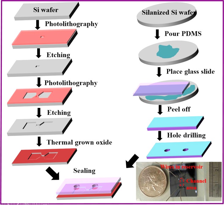
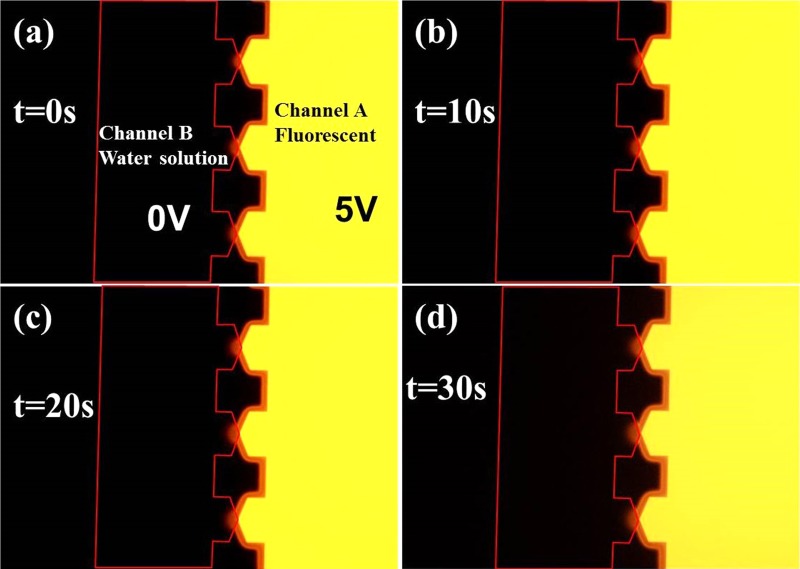
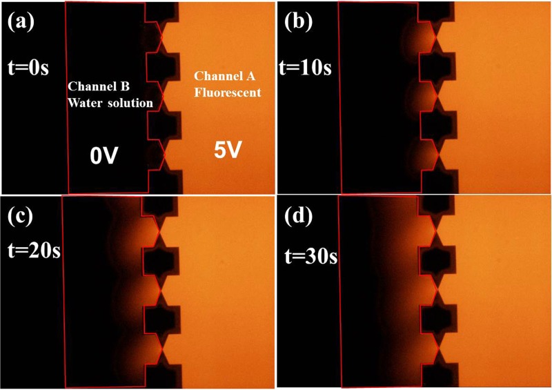
Electrodeless dielectrophoresis is the best choice to achieve preconcentration of nanoparticles and biomolecules due to its simple, robust, and easy implementation. We designed a simple chip with microchannels and nano-slits in between and then studied the trapping of DNA in high conductive medium and low conductive medium, corresponding to positive and negative dielectrophoresis (DEP), respectively. It is very important to investigate the trapping in media with different conductivities since one always has to deal with the sample solutions with different conductivities. The trapping process was analyzed by the fluorescent intensity changes. The results showed that DNA could be trapped at the nano-slit in both high and low conductive media in a lower electric field strength (10 V/cm) compared to the existing methods. This is a significant improvement to suppress the Joule heating effect in DEP related experiments. Our work may give insight to researchers for DNA trapping by a simple and low cost device in the Lab-on-a-Chip system.
Figures


Similar articles
-
Electric field-induced effects on neuronal cell biology accompanying dielectrophoretic trapping.Adv Anat Embryol Cell Biol. 2003;173:III-IX, 1-77. doi: 10.1007/978-3-642-55469-8. Adv Anat Embryol Cell Biol. 2003. PMID: 12901336 Review.
-
Scaling down constriction-based (electrodeless) dielectrophoresis devices for trapping nanoscale bioparticles in physiological media of high-conductivity.Electrophoresis. 2013 Apr;34(7):1097-104. doi: 10.1002/elps.201200456. Epub 2013 Mar 11. Electrophoresis. 2013. PMID: 23436401
-
Theoretical and experimental analysis of negative dielectrophoresis-induced particle trajectories.Electrophoresis. 2022 Jun;43(12):1366-1377. doi: 10.1002/elps.202100372. Epub 2022 May 15. Electrophoresis. 2022. PMID: 35377504 Free PMC article.
-
Electrodeless dielectrophoresis: Impact of geometry and material on obstacle polarization.Electrophoresis. 2016 Jan;37(2):291-301. doi: 10.1002/elps.201500313. Epub 2015 Nov 23. Electrophoresis. 2016. PMID: 26463845
-
A correlation of conductivity medium and bioparticle viability on dielectrophoresis-based biomedical applications.Electrophoresis. 2023 Mar;44(5-6):573-620. doi: 10.1002/elps.202200203. Epub 2023 Jan 16. Electrophoresis. 2023. PMID: 36604943 Review.
Cited by
-
Hybridization-based DNA biosensing with a limit of detection of 4 fM in 30 s using an electrohydrodynamic concentration module fabricated by grayscale lithography.Biomicrofluidics. 2022 Aug 16;16(4):044111. doi: 10.1063/5.0073542. eCollection 2022 Jul. Biomicrofluidics. 2022. PMID: 35992636 Free PMC article.
-
Preconcentration of diluted mixed-species samples following separation and collection in a micro-nanofluidic device.Biomicrofluidics. 2016 Feb 18;10(1):014119. doi: 10.1063/1.4942037. eCollection 2016 Jan. Biomicrofluidics. 2016. PMID: 26909125 Free PMC article.
References
-
- Hardin J. O. and Milam V. T., Soft Matter 7, 2674 (2011).10.1039/c0sm00942c - DOI
LinkOut - more resources
Full Text Sources
Other Literature Sources
Miscellaneous