

Self-aligned, full solution process polymer field-effect transistor on flexible substrates
- PMID: 26497412
- PMCID: PMC4620563
- DOI: 10.1038/srep15770
Self-aligned, full solution process polymer field-effect transistor on flexible substrates
Abstract
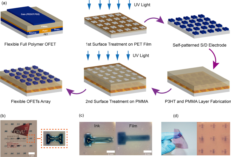
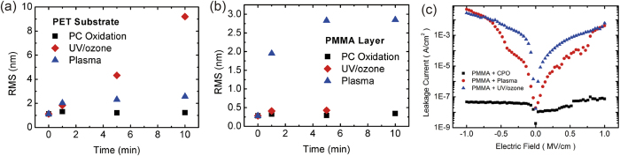
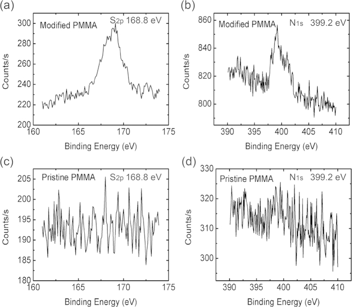
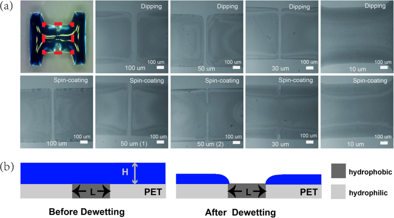
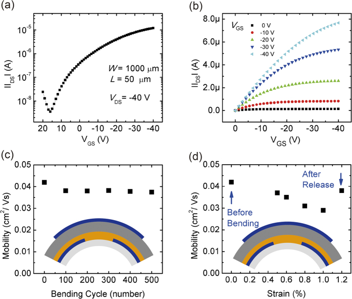
Conventional techniques to form selective surface energy regions on rigid inorganic substrates are not suitable for polymer interfaces due to sensitive and soft limitation of intrinsic polymer properties. Therefore, there is a strong demand for finding a novel and compatible method for polymeric surface energy modification. Here, by employing the confined photo-catalytic oxidation method, we successfully demonstrate full polymer filed-effect transistors fabricated through four-step spin-coating process on a flexible polymer substrate. The approach shows negligible etching effect on polymeric film. Even more, the insulating property of polymeric dielectric is not affected by the method, which is vital for polymer electronics. Finally, the self-aligned full polymer field-effect transistors on the flexible polymeric substrate are fabricated, showing good electrical properties and mechanical flexibility under bending tests.
Figures
Similar articles
-
Surface Decoration on Polymeric Gate Dielectrics for Flexible Organic Field-Effect Transistors via Hydroxylation and Subsequent Monolayer Self-Assembly.ACS Appl Mater Interfaces. 2015 Oct 28;7(42):23464-71. doi: 10.1021/acsami.5b05363. Epub 2015 Oct 13. ACS Appl Mater Interfaces. 2015. PMID: 26439239
-
Self-aligned, vertical-channel, polymer field-effect transistors.Science. 2003 Mar 21;299(5614):1881-4. doi: 10.1126/science.1081279. Science. 2003. PMID: 12649478
-
Highly transparent and flexible nanopaper transistors.ACS Nano. 2013 Mar 26;7(3):2106-13. doi: 10.1021/nn304407r. Epub 2013 Feb 7. ACS Nano. 2013. PMID: 23350951
-
Flexible Organic Transistors with Controlled Nanomorphology.Nano Lett. 2016 Jan 13;16(1):314-9. doi: 10.1021/acs.nanolett.5b03868. Epub 2015 Dec 14. Nano Lett. 2016. PMID: 26645364
-
A review of fabrication and applications of carbon nanotube film-based flexible electronics.Nanoscale. 2013 Mar 7;5(5):1727-52. doi: 10.1039/c3nr33560g. Epub 2013 Feb 5. Nanoscale. 2013. PMID: 23381727 Review.
Cited by
-
In vitro and in vivo studies on the biocompatibility of a self-powered pacemaker with a flexible buckling piezoelectric vibration energy harvester for rats.Ann Transl Med. 2021 May;9(9):800. doi: 10.21037/atm-21-1707. Ann Transl Med. 2021. PMID: 34268413 Free PMC article.
-
Interface studies of well-controlled polymer bilayers and field-effect transistors prepared by a mixed-solvent method.RSC Adv. 2018 Mar 21;8(21):11272-11279. doi: 10.1039/c7ra13143g. eCollection 2018 Mar 21. RSC Adv. 2018. PMID: 35542823 Free PMC article.
References
-
- Liu S., Wang W. M., Briseno A. L., Mannsfeld S. C. B. & Bao Z. Controlled deposition of crystalline organic semiconductors for field-effect-transistor applications. Adv. Mater. 21, 1217–1232 (2009).
-
- Sirringhaus H. Device physics of solution-processed organic field-effect transistors. Adv. Mater. 17, 2411–2425 (2005).
-
- Guo Y., Yu G. & Liu Y. Functional organic field-effect transistors. Adv. Mater. 22, 4427–4447 (2010). - PubMed
-
- Yan Y. et al. Probing bias stress effect and contact resistance in bilayer ambipolar organic field-effect transistors. Appl. Phys. Lett. 103, 073303 (2013).
-
- Yan Y., She X. J., Zhu H. & Wang S. D. Origin of bias stress induced instability of contact resistance in organic thin film transistors. Org. Electron. 12, 823–826. (2011).
Publication types
LinkOut - more resources
Full Text Sources
Other Literature Sources
