

Planar-integrated single-crystalline perovskite photodetectors
- PMID: 26548941
- PMCID: PMC4667636
- DOI: 10.1038/ncomms9724
Planar-integrated single-crystalline perovskite photodetectors
Abstract
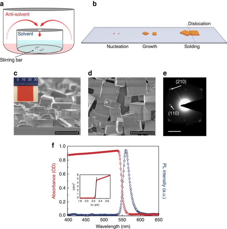
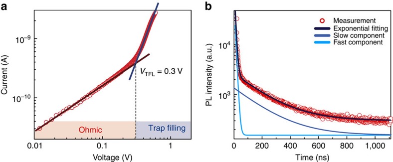
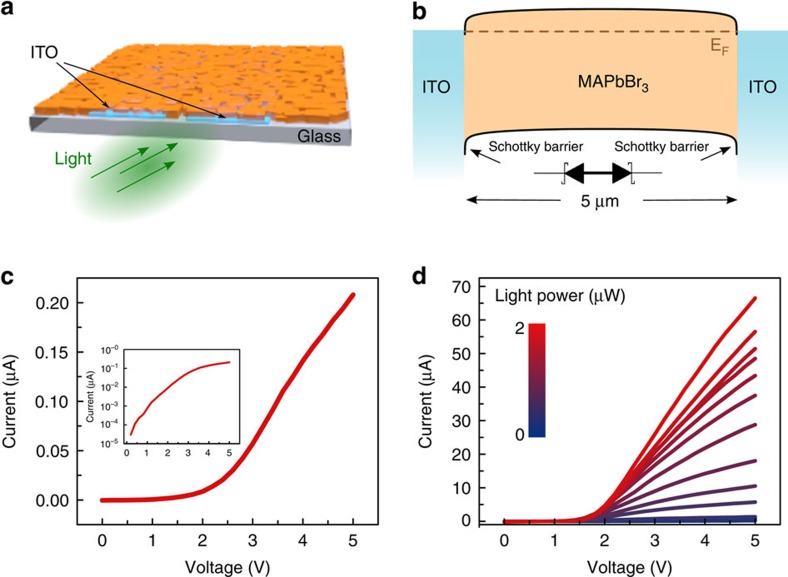
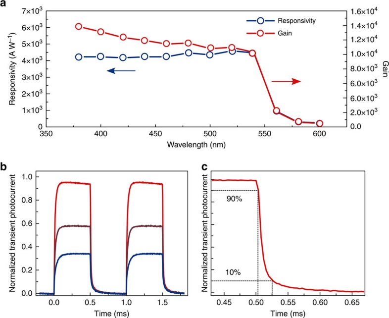
Hybrid perovskites are promising semiconductors for optoelectronic applications. However, they suffer from morphological disorder that limits their optoelectronic properties and, ultimately, device performance. Recently, perovskite single crystals have been shown to overcome this problem and exhibit impressive improvements: low trap density, low intrinsic carrier concentration, high mobility, and long diffusion length that outperform perovskite-based thin films. These characteristics make the material ideal for realizing photodetection that is simultaneously fast and sensitive; unfortunately, these macroscopic single crystals cannot be grown on a planar substrate, curtailing their potential for optoelectronic integration. Here we produce large-area planar-integrated films made up of large perovskite single crystals. These crystalline films exhibit mobility and diffusion length comparable with those of single crystals. Using this technique, we produced a high-performance light detector showing high gain (above 10(4) electrons per photon) and high gain-bandwidth product (above 10(8) Hz) relative to other perovskite-based optical sensors.
Figures
References
-
- Tan Z.-K. et al.. Bright light-emitting diodes based on organometal halide perovskite. Nat. Nanotechnol. 9, 687–692 (2014). - PubMed
-
- Li G. et al.. Efficient light-emitting diodes based on nano-crystalline perovskite in a dielectric polymer matrix. Nano Lett. 15, 2640–2644 (2015). - PubMed
-
- Dou L. et al.. Solution-processed hybrid perovskite photodetectors with high detectivity. Nat. Commun. 5, 5404 (2014). - PubMed
-
- Yang W. S. et al.. High-performance photovoltaic perovskite layers fabricated through intermolecular exchange. Science 348, 1234–1237 (2015). - PubMed
-
- Snaith H. J. Perovskites: the emergence of a new era for low-cost, high-efficiency solar cells. J. Phys. Chem. Lett. 4, 3623–3630 (2013).
Publication types
LinkOut - more resources
Full Text Sources
Other Literature Sources
