

Substrate-Free InGaN/GaN Nanowire Light-Emitting Diodes
- PMID: 26577391
- PMCID: PMC4648807
- DOI: 10.1186/s11671-015-1143-5
Substrate-Free InGaN/GaN Nanowire Light-Emitting Diodes
Abstract
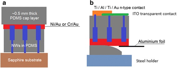
We report on the demonstration of substrate-free nanowire/polydimethylsiloxane (PDMS) membrane light-emitting diodes (LEDs). Metal-organic vapour-phase epitaxy (MOVPE)-grown InGaN/GaN core-shell nanowires were encapsulated into PDMS layer. After metal deposition to p-GaN, a thick PDMS cap layer was spin-coated and the membrane was manually peeled from the sapphire substrate, flipped upside down onto a steel holder, and transparent indium tin oxide (ITO) contact to n-GaN was deposited. The fabricated LEDs demonstrate rectifying diode characteristics. For the electroluminescence (EL) measurements, the samples were manually bonded using silver paint. The EL spectra measured at different applied voltages demonstrate a blue shift with the current increase. This shift is explained by the current injection into the InGaN areas of the active region with different average indium content.
Keywords: Light-emitting diodes; Nanowire; Substrate-free devices Gallium nitride.
Figures


References
-
- Li S, Waag A. GaN based nanorods for solid state lighting. J Appl Phys. 2012
-
- Shirasaki Y, Supran GJ, Bawendi MG, Bulovic V. Emergence of colloidal quantum-dot light-emitting technologies. Nat Photonics. 2013
-
- Kang MS, Lee CH, Park JB, Yoo H, Yi GC. Gallium nitride nanostructures for light-emitting diode applications. Nano Energy. 2012
-
- Foltynski B, Giesen C, Heuken M. Self-organized growth of catalyst-free GaN nano-and micro-rods on Si (111) substrates by MOCVD. Phys Status Solidi B. 2015
LinkOut - more resources
Full Text Sources
Other Literature Sources
Miscellaneous
