. 2015 Nov 30:6:10030.
doi: 10.1038/ncomms10030.

Enhanced optoelectronic quality of perovskite thin films with hypophosphorous acid for planar heterojunction solar cells

Affiliations

Enhanced optoelectronic quality of perovskite thin films with hypophosphorous acid for planar heterojunction solar cells

Wei Zhang et al. Nat Commun. .

Abstract

Solution-processed metal halide perovskite semiconductors, such as CH3NH3PbI3, have exhibited remarkable performance in solar cells, despite having non-negligible density of defect states. A likely candidate is halide vacancies within the perovskite crystals, or the presence of metallic lead, both generated due to the imbalanced I/Pb stoichiometry which could evolve during crystallization. Herein, we show that the addition of hypophosphorous acid (HPA) in the precursor solution can significantly improve the film quality, both electronically and topologically, and enhance the photoluminescence intensity, which leads to more efficient and reproducible photovoltaic devices. We demonstrate that the HPA can reduce the oxidized I2 back into I(-), and our results indicate that this facilitates an improved stoichiometry in the perovskite crystal and a reduced density of metallic lead.


Figures
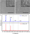
Figure 1
Figure 1. Morphological and crystallographic analysis.
SEM images for the perovskite thin films deposited on compact TiO2 (c-TiO2) coated FTO glass prepared from the precursor solution without (a) and with (b) HPA, with scale bars of 20 μm in the images and 1 μm in the insets, and corresponding XRD spectra (c). Note that the scattering peak from PbI2 impurity, denoted #, is absent from the material processed with HPA.
Figure 2
Figure 2. Photophysical properties of the perovskite films.
(a) UV–vis absorption spectra of ∼200-nm-thick perovskite thin films coated on glass substrates prepared from the precursor solution without (control) and with HPA. (b) PDS spectra of the perovskite film without and with HPA deposited on quartz substrate. The inset shows the average Urbach energies for these samples with s.d. (c) Steady-state and (d) time-resolved photoluminescence (PL) spectra for the perovskite thin films deposited on glass prepared from the precursor solution without (control) and with HPA. Grey lines are the model fits (Supplementary Note 1).
Figure 3
Figure 3. Fluorescence microscopy analysis.
(a) A 10 × 10 μm fluorescence image (FI) of a control perovskite film on glass and (d) a perovskite film formed with HPA additive. (a,d) Scale bar, 2 μm. (b) Image histogram of FI in (a) fitted to a Gaussian function (black trace) and ((e), top) histogram of FI in (d) fitted to a sum (black trace) of two Gaussian functions (blue and red traces, (e) bottom). (c,f) Time-resolved PL decay curves of bright (red square), medium (green triangle), and dark (blue circle) PL intensity regions after excitation at 470 nm, 500 kHz, ϕ=1 μJ cm−2.
Figure 4
Figure 4. Kelvin probe measurements.
(a) Schematic band diagram for the generation of surface photovoltage (SPV) at the perovskite surface (CBM, conduction band minimum, VBM, valence band maximum). The solid lines and the dotted lines represent the condition in the dark and light, respectively. (b) Surface work function of perovskite films on FTO as a function of light intensity; control perovskite film shows a decrease in work function by 430 mV, whereas the HPA-modified sample shows a decrease of 210 mV only due to lower density of surface states. The work function of the kelvin probe was calibrated by a freshly cleaved highly ordered pyrolytic graphite surface, which has known work function of 4.65 eV (ref. 47).
Figure 5
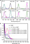
Figure 5. The possible origin of electronic trap states.
(a) The high-resolution XPS spectra of Pb 4f and I 3d detail spectra for the perovskite films deposited on c-TiO2 coated FTO glass prepared from the precursor solution without (control) and with HPA. Peak pertaining to unsaturated Pb has been marked with star in the figure, which becomes smaller after addition of HPA in the precursor. (b) Ultraviolet–visible (UV–vis) absorption spectra of MAI or I2 dissolved in DMF and absorption quenching of MAI solution by adding HPA.

References

    1. Kojima A., Teshima K., Shirai Y. & Miyasaka T. Organometal halide perovskites as visible-light sensitizers for photovoltaic cells. J. Am. Chem. Soc. 131, 6050–6051 (2009). - PubMed
    1. Lee M. M., Teuscher J., Miyasaka T., Murakami T. N. & Snaith H. J. Efficient hybrid solar cells based on meso-superstructured organometal halide perovskites. Science 338, 643–647 (2012). - PubMed
    1. Kim H.-S. et al.. Lead iodide perovskite sensitized all-solid-state submicron thin film mesoscopic solar cell with efficiency exceeding 9%. Sci. Rep. 2, 591 (2012). - PMC - PubMed
    1. Tan Z.-K. et al.. Bright light-emitting diodes based on organometal halide perovskite. Nat. Nanotechnol. 9, 687–692 (2014). - PubMed
    1. Yang W. S. et al.. High-performance photovoltaic perovskite layers fabricated through intramolecular exchange. Science 348, 1234–1237 (2015). - PubMed

Publication types