. 2015 Nov 30:5:17377.
doi: 10.1038/srep17377.

Electric-field-assisted formation of an interfacial double-donor molecule in silicon nano-transistors

Affiliations

Electric-field-assisted formation of an interfacial double-donor molecule in silicon nano-transistors

Arup Samanta et al. Sci Rep. .

Abstract

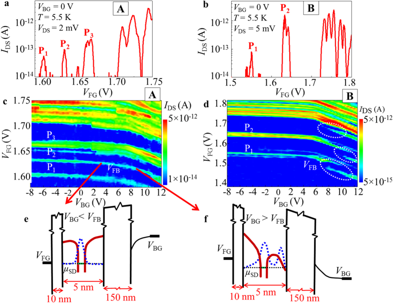
Control of coupling of dopant atoms in silicon nanostructures is a fundamental challenge for dopant-based applications. However, it is difficult to find systems of only a few dopants that can be directly addressed and, therefore, experimental demonstration has not yet been obtained. In this work, we identify pairs of donor atoms in the nano-channel of a silicon field-effect transistor and demonstrate merging of the donor-induced potential wells at the interface by applying vertical electric field. This system can be described as an interfacial double-donor molecule. Single-electron tunneling current is used to probe the modification of the potential well. When merging occurs at the interface, the gate capacitance of the potential well suddenly increases, leading to an abrupt shift of the tunneling current peak to lower gate voltages. This is due to the decrease of the system's charging energy, as confirmed by Coulomb blockade simulations. These results represent the first experimental observation of electric-field-assisted formation of an interfacial double-donor molecule, opening a pathway for designing functional devices using multiple coupled dopant atoms.


Figures

Figure 1
Figure 1. Ultrathin silicon-on-insulator field-effect transistors.
(a) Schematic structure of an SOI-FET and its measurement setup. (b) A SEM image of a typical channel with dimensions below 100 nm. (c) TEM image of the channel taken across the channel width. (d) Schematic illustration of a possible arrangement of P-donors in a randomly, lower-concentration-doped channel. Under vertical electric field, potential wells can be formed at the interface. Neighboring potential wells may merge forming an interfacial double-donor molecule. (e) Schematic illustration of a possible distribution of P-donors in a selectively-doped higher-concentration channel. Clusters of several P-donors are located in the central region of the channel, strongly interacting to form multiple-donor QDs.
Figure 2
Figure 2. Vertical electric field effect.
(a,b) IDSVFG characteristics (VDS = 2 mV and 5 mV, respectively; T = 5.5 K) measured for two different SOI-MOSFETs with channels randomly doped (ND ≈ 1 × 1018 cm−3). Noise level in these measurements in ~10 fA (shown as cut off level for the vertical axes). (c,d) Contour plots of IDS as a function of backgate voltage (VBG) and frontgate voltage (VFG) for devices A and B, respectively. Device A shows relatively smooth current traces, while device B shows sudden changes in the current peak positions at positive VBG. (e,f) Illustrations of the energy band diagrams and of the electron wave functions at electric fields corresponding to below and above the flatband condition. μSD is source-drain chemical potential.
Figure 3
Figure 3. Calculation of probability of donor-well merging.
(a,b) Number of isolated and merged dopant-induced wells calculated probabilistically as a function of electric field for two different distances of P-donors from the back interface: 3.8 nm [(a)] and 2.7 nm [(b)]. Insets: number of systems in the device channel containing 2, 3, or 4 merged P-donor wells assuming a Poisson distribution of the P-donors. The green zones correspond to the range of electric fields estimated for our experiment.
Figure 4
Figure 4. Transport characteristics for devices doped with lower and higher concentration.
Contour plots of IDS (top panels) and d2IDS/dVFG2 (bottom panels) as a function of backgate voltage (VBG) and frontgate voltage (VFG) for two types of devices: (a,b) randomly doped with lower doping concentration (ND ≈ 1 × 1018 cm−3); (c,d) selectively-doped with higher doping concentration (ND > 1 × 1019 cm−3). All data is measured at T = 5.5 K and VDS = 5 mV. Regions of current shifts are marked by dashed rectangles in (a,b). IDSVFG characteristics (VBG = 0 V) for the selectively-doped high-concentration FET are shown as a side panel in (c). In (d), within the complex pattern of fine traces, several anti-crossing structures are marked by dashed lines, suggesting interaction between two QDs. Zoom-in plots of two such regions [marked as (i) and (ii)] are presented in the right-side panels of (d).
Figure 5
Figure 5. Transport mechanism and Coulomb blockade simulation of merging donor-wells.
(a) Schematic representation of the evolution of one main current peak (P1) with increasing VBG. P′1 corresponds to a fine current trace due to a satellite neighboring P-donor. Insets: potential landscapes of a double-donor system (with donors located at 3.8 nm and 4.5 nm, respectively, from the back interface) for different vertical electric fields (Fz). Three different regimes are shown: (i) Fz = 0 mV/nm; (ii) Fz–low; (iii) Fz–high. (b) Equivalent circuit of two parallel-coupled donor-induced QDs. (c) Equivalent circuit of two parallel-coupled donor-well QDs with increasing gate capacitance due to the gradual expansion of the donor-wells at the interface. (d) Equivalent circuit of merged two-donor-well (forming a single QD with larger gate capacitance). (e) Simulated IDS plotted in the VFG-VBG plane, as obtained for the sequence of equivalent circuits shown in (bd).

References

    1. Mizuno T., Okamura J & Toriumi A. Experimental study of threshold voltage fluctuation due to statistical variation of channel dopant number in MOSFET’s. IEEE Trans. Electron Devices 41, 2216–2221 (1994).
    1. Roy S. & Asenov A. Where Do the Dopants Go? Science 309, 388–390 (2005). - PubMed
    1. Shinada T., Okamoto S., Kobayashi T. & Ohdomari I. Enhancing semiconductor device performance using ordered dopant arrays. Nature 437, 1128–1131 (2005). - PubMed
    1. Prati E., Hori M., Guagliardo F., Ferrari G. & Shinada T. Anderson–Mott transition in arrays of a few dopant atoms in a silicon transistor. Nat. Nanotechnol. 7, 443–447 (2012). - PubMed
    1. Pierre M., et al. Single-donor ionization energies in a nanoscale CMOS channel. Nat. Nanotechnol. 5, 133–137 (2010). - PubMed

Publication types

LinkOut - more resources