Review
. 2016 Jan 13;116(1):215-57.
doi: 10.1021/acs.chemrev.5b00608. Epub 2015 Dec 21.

Nano-Bioelectronics

Affiliations
Review

Nano-Bioelectronics

Anqi Zhang et al. Chem Rev. .

Abstract

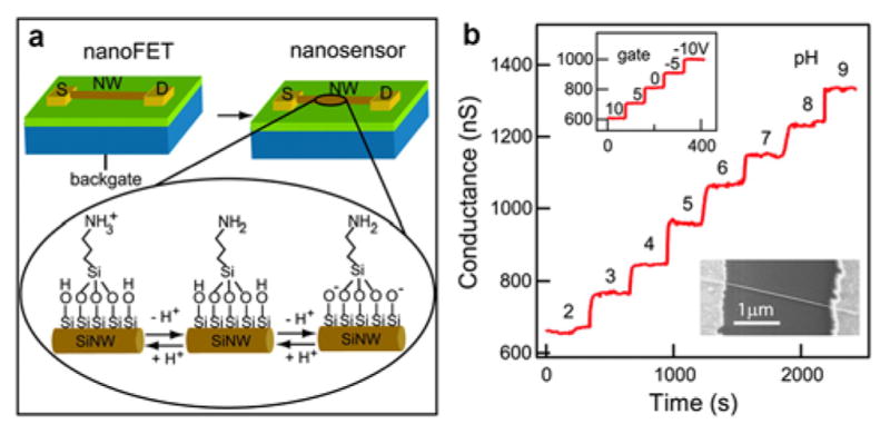
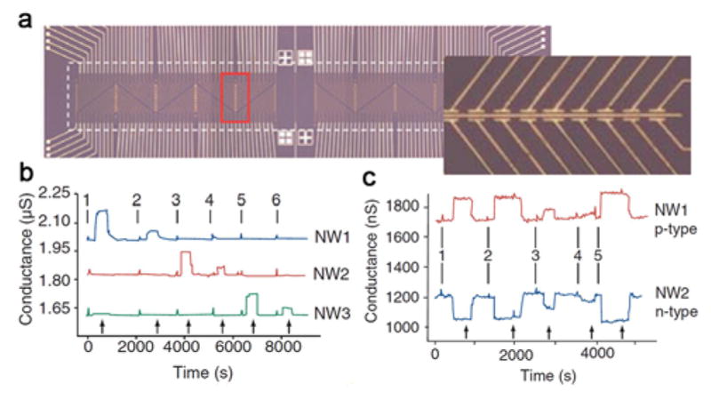
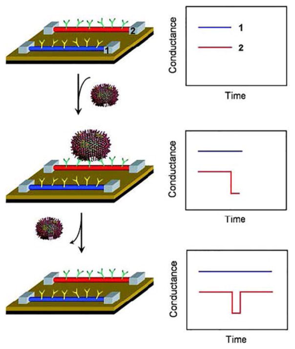
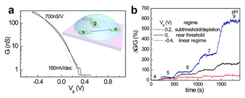
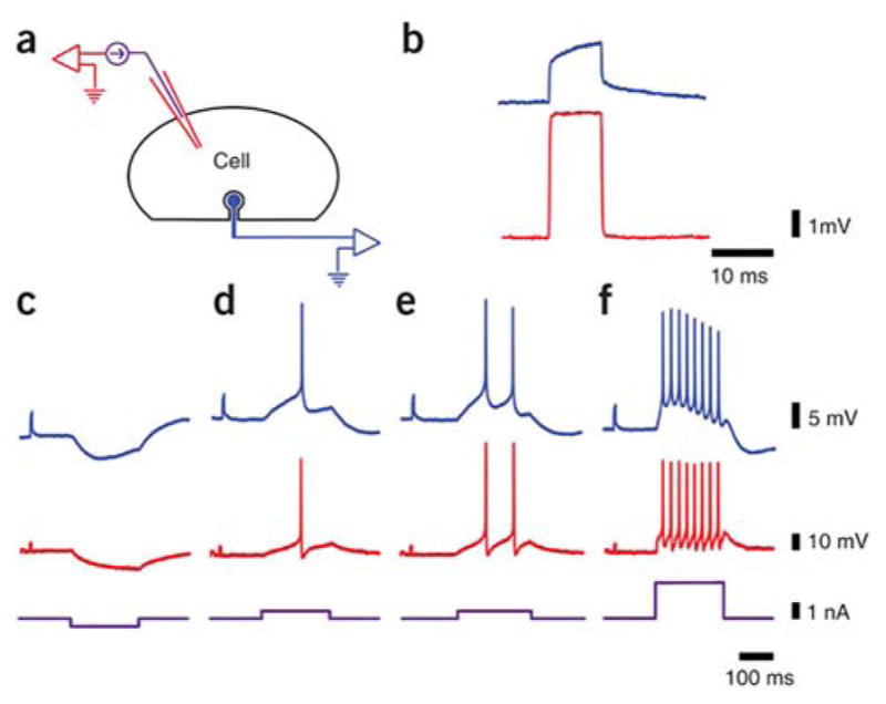
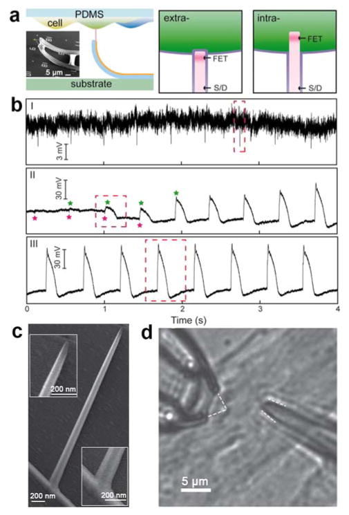
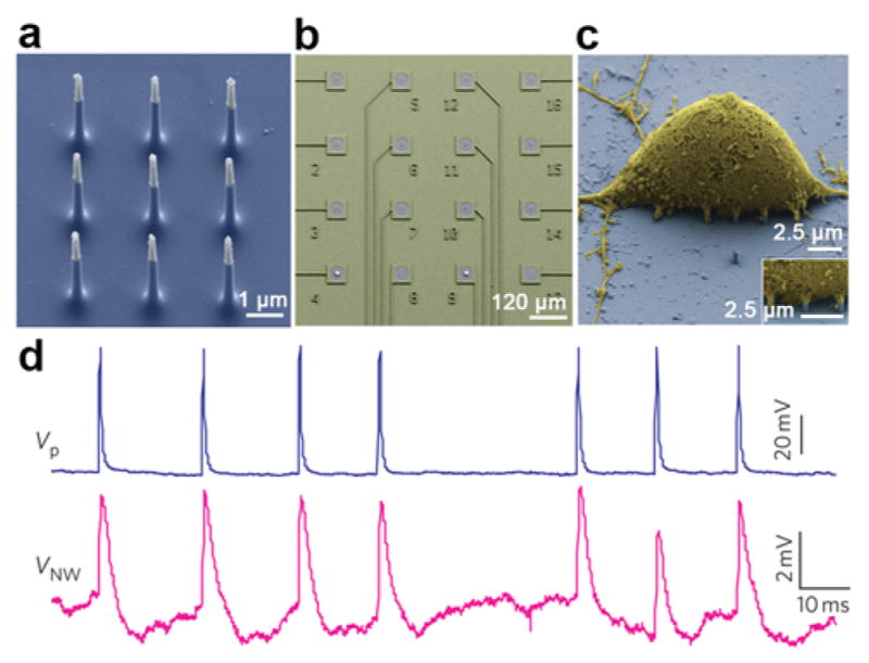
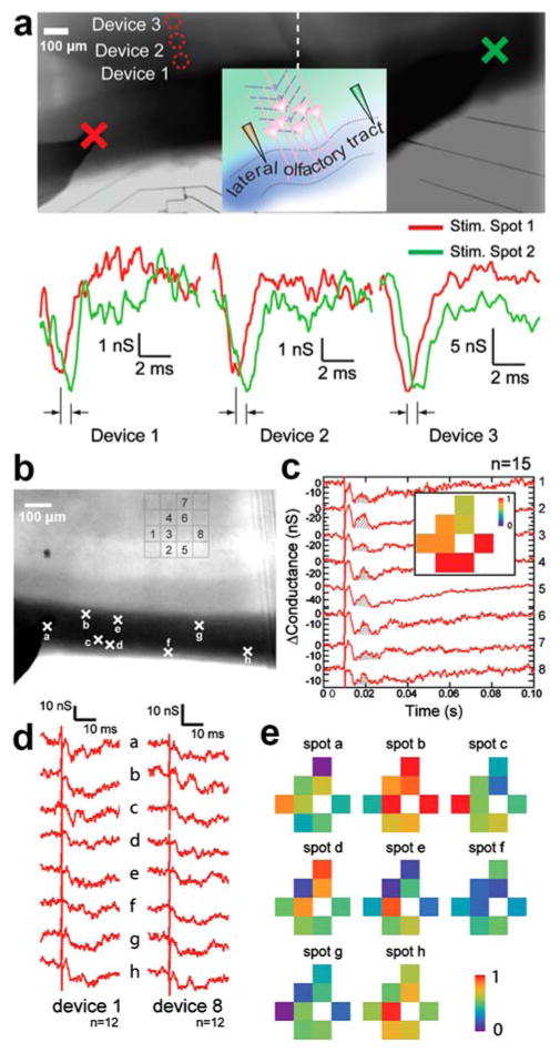
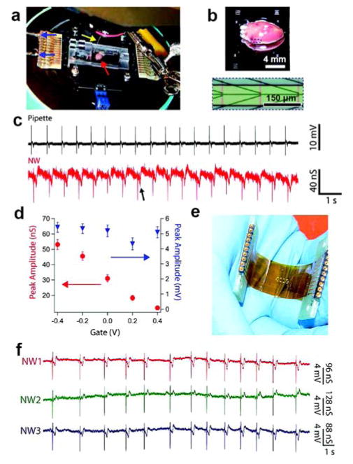
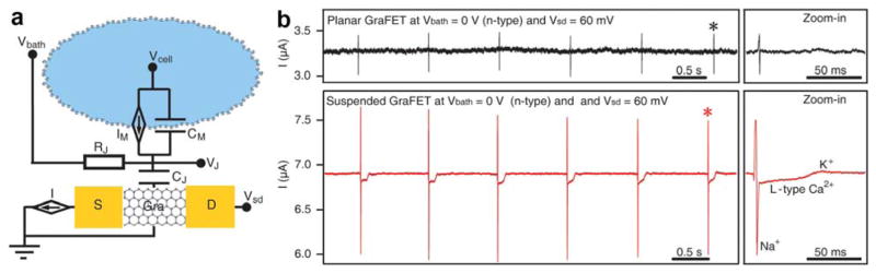
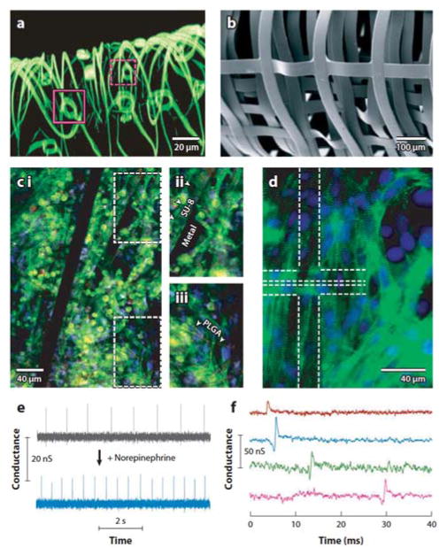
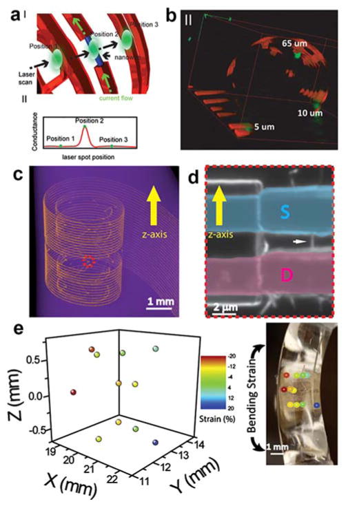
Nano-bioelectronics represents a rapidly expanding interdisciplinary field that combines nanomaterials with biology and electronics and, in so doing, offers the potential to overcome existing challenges in bioelectronics. In particular, shrinking electronic transducer dimensions to the nanoscale and making their properties appear more biological can yield significant improvements in the sensitivity and biocompatibility and thereby open up opportunities in fundamental biology and healthcare. This review emphasizes recent advances in nano-bioelectronics enabled with semiconductor nanostructures, including silicon nanowires, carbon nanotubes, and graphene. First, the synthesis and electrical properties of these nanomaterials are discussed in the context of bioelectronics. Second, affinity-based nano-bioelectronic sensors for highly sensitive analysis of biomolecules are reviewed. In these studies, semiconductor nanostructures as transistor-based biosensors are discussed from fundamental device behavior through sensing applications and future challenges. Third, the complex interface between nanoelectronics and living biological systems, from single cells to live animals, is reviewed. This discussion focuses on representative advances in electrophysiology enabled using semiconductor nanostructures and their nanoelectronic devices for cellular measurements through emerging work where arrays of nanoelectronic devices are incorporated within three-dimensional cell networks that define synthetic and natural tissues. Last, some challenges and exciting future opportunities are discussed.


Conflict of interest statement

Notes

The authors declare no competing financial interest.

Figures

Figure 1
Figure 1
VLS growth mechanism of SiNWs.
Figure 2
Figure 2
Five classes of NW structures available today: basic (center), axial, core/shell, branched and kinked structures, clockwise from lower left. Reprinted with permission from Ref. . Copyright 2011 Materials Research Society.
Figure 3
Figure 3
(a) Schematic for flow-assisted alignment of parallel NW arrays. (b, c) Schematic and SEM images of crossed NW matrix obtained by changing the flow direction sequentially. (d) A triangle of NWs obtained in a three-step assembly process. Reprinted with permission from Ref. . Copyright 2001 American Association for the Advancement of Science. (e) Contact printing of NWs. (f) 3D NW circuit fabricated by multiple contact printing steps. Reprinted with permission from Ref. . Copyright 2007 American Chemical Society.
Figure 4
Figure 4
(a) Schematics of the nanocombing process. (b, c) SEM images of SiNWs on the combing surface. Reprinted with permission from Ref. . Copyright 2013 Nature Publishing Group.
Figure 5
Figure 5
(a) A typical planar FET. The semiconductor substrate (e.g., p-Si) is connected to gate (G), source (S) and drain (D) electrodes, and can be switches between the “off” and “on” states by applying the Vg. (b) Schematic and SEM image of a NW-FET. Reprinted with permission from Ref. . Copyright 2002 American Chemical Society. (c, d) Transistor characteristics of p- and n-type NWs. Insets show transfer characteristics of the back-gated devices. (c) Reprinted with permission from Ref. . Copyright 2004 American Chemical Society. (d) Reprinted with permission from Ref. . Copyright 2004 John Wiley & Sons, Inc.
Figure 6
Figure 6
Schemes for synthesis of SWNTs with single chirality. (a) Preparation of the W–Co catalyst and the growth of a SWNT. (b) UV–Vis–NIR spectrum from 42 samples. (c) Relative abundances of various chiralities from ~3,300 nanotubes. Reprinted with permission from Ref. . Copyright 2014 Nature Publishing Group. (d) Formation of singly capped ultrashort (6,6) seed and subsequent elongation of SWNT. Reprinted with permission from Ref. . Copyright 2014 Nature Publishing Group.
Figure 7
Figure 7
(a) Mechanically exfoliated single-layer graphene sheet. Reprinted with permission from Ref. . Copyright 2004 American Association for the Advancement of Science. (b) Liquid-phase exfoliated two-layer graphene LB film on quartz. (c) Transparency spectra of one- (black), two- (red) and three-layer (green) LB films. Reprinted with permission from Ref. . Copyright 2008 Nature Publishing Group. (d) Large-area graphene grown by CVD on copper substrate spanning 30 inches diagonally. Reprinted with permission from Ref. . Copyright 2010 Nature Publishing Group. (e) AFM image of epitaxial graphene grown on SiC. Reprinted with permission from Ref. . Copyright 2009 Nature Publishing Group. (f) STM image of synthesized graphene nanoribbons. Reprinted with permission from Ref. . Copyright 2010 Nature Publishing Group.
Figure 8
Figure 8
Schematic comparison of (top) a standard FET device and (bottom) a SiNW FET sensor. The NW surface is functionalized with a receptor layer to recognize target biomolecules in a solution, which are charged and provide a molecular gating effect on SiNWs. Reprinted with permission from Ref. . Copyright 2006 Future Medicine Ltd.
Figure 9
Figure 9
(a) Schematic of a functionalized NW device and the protonation/deprotonation process that changes the surface charge state. (b) Changes in NW conductance versus pH. Reprinted with permission from Ref. . Copyright 2001 American Association for the Advancement of Science.
Figure 10
Figure 10
(a) Optical image of a NW array. (b) Sequential detection of PSA, CEA and mucin–1 solutions using three SiNW FET sensors. (c) Complementary sensing of PSA using p–type (NW1) and n–type (NW2) SiNW FET sensors. Reprinted with permission from Ref. . Copyright 2005 Nature Publishing Group.
Figure 11
Figure 11
Schematic of virus binding/unbinding to a SiNW FET and the corresponding time–dependent conductance change. Reprinted with permission from Ref. . Copyright 2004 National Academy of Sciences of the United States of America.
Figure 12
Figure 12
(a) Conductance, G, vs Vg for a p-type SiNW FET. Inset: scheme for electrolyte gating. (b) Real time pH sensing. The device in the subthreshold regime shows much larger ΔG/G change versus pH. Reprinted with permission from Ref. . Copyright 2010 American Chemical Society.
Figure 13
Figure 13
(a) Electrical noise in a time–domain measurement. (b) Lorentzian and 1/f functions in the frequency domain. (c) Models of a two–level system (left) and RC circuit (right). Reprinted with permission from Ref. . Copyright 2010 American Chemical Society.
Figure 14
Figure 14
(a, b) Schematic and TEM image of a SiNW-nanopore sensor. (c) Recording of SiNW-nanopore FET conductance and ionic current during DNA translocation. Reprinted with permission from Ref. . Copyright 2012 Nature Publishing Group.
Figure 15
Figure 15
(a) Schematic of a polymer–biotin functionalized SWNT-FET for streptavidin recognition. (b) I-Vg relationship before and after adding streptavidin. Reprinted with permission from Ref. . Copyright 2003 American Chemical Society.
Figure 16
Figure 16
(a) Conductance versus time monitoring various BSA concentrations. Reprinted with permission from Ref. . Copyright 2009 American Chemical Society. (b) Schematic of a graphene FET device based on rGO for detection of IgG. IgG antibodies are anchored on AuNPs. Reprinted with permission from Ref. . Copyright 2010 John Wiley & Sons, Inc. (c) Real-time detection of fibronection using the all-rGO sensor. Reprinted with permission from Ref. . Copyright 2011 American Chemical Society.
Figure 17
Figure 17
(a) Optical image of a NW-neuron interface. (b) Neuron stimulation and resulting NW electrical responses. NW4 is not in contact with any neurites. (c) Propagation studies using the multi-NW–neurite structures. Top: Optical image of the settings. Bottom: Relation of latency time with distance and histogram of propagation speed. (d) Aligned axon crossing a 50-NW device array and corresponding signal propagation data. Reprinted with permission from Ref. . Copyright 2006 American Association for the Advancement of Science.
Figure 18
Figure 18
Interfacing SiNW FETs with cardiomyocytes for extracellular recording. (a) Long NWs fabricated by top-down paradigm. Isolated cardiomyocytes are cultured on the NW chip, where the dark lines denoted two NWs, I and II. (b) Currents measured by NW I and II. A series of transient current events are observed for NW II because it is covered by a contracting myocyte. (c) Typical results from NW II (left) compared to the intracellular action potential recorded with a nanopipette (Right). Reprinted with permission from Ref. . Copyright 2009 John Wiley & Sons, Inc. (d, e) Schematic of a cardiomyocyte on a NW-FET device and the displacement (Z) of the PDMS/cell substrate. (f) Two traces recorded with different Z values. Reprinted with permission from Ref. . Copyright 2009 National Academy of Sciences of the United States of America. (g) Point-like recording using a short-channel NW fabricated by bottom-up paradigm. Left: Schematic of the short-channel FET-cell interface, where the active channel size is comparable to that of a few ion channels. Right: Typical signals of beating cardiomyocytes from devices with channel lengths of 150 (blue), 80 (green) and 50 nm (red). Reprinted with permission from Ref. . Copyright 2012 American Chemical Society.
Figure 19
Figure 19
SiNW interfaced to aortic smooth muscle cells. (a) Rat aortic smooth muscle cells (A7r5) on the NW chip, in which the dashed square depicts the sensing area. (b) NW recorded current signals induced by membrane depolarizing in high concentration K+ solution. Reprinted with permission from Ref. . Copyright 2009 John Wiley & Sons, Inc.
Figure 20
Figure 20
Extracellular recording using graphene FETs. (a) Schematic illustrating cardiomyocyte cell interfaced to graphene- and SiNW-FET devices. (b) Recorded extracellular spikes versus gate potential. (c) Summary of the gate potential versus conductance change and calibrated voltage. Reprinted with permission from Ref. . Copyright 2010 American Chemical Society. (d) Schematic of a cell on a graphene-FET. (e) Typical two- and one-side peaks observed for different transistors. (f) Simultaneous current recordings from eight transistors in one FET array over hundreds of milliseconds. Reprinted with permission from Ref. . Copyright 2011 John Wiley & Sons, Inc.
Figure 21
Figure 21
Intracellular-like recordings with FGSEs. (a) Experimental setup with one cell interfaced to a single glass microelectrode (red) and FGSE (blue). (b) Calibrated recording from the intracellular microelectrode (red) and FGSE (blue) for a pulse of 5 mV, 20 ms, (c) A hyperpolarizing current pulse (purple) induced hyperpolarization recorded by the intracellular microelectrode (red) and the FGSE (blue). (d–f) Depolarizing currents generated action potentials with amplitudes of ~50 mV (intracellular microelectrode, red) and ~25 mV (FGSE, blue). Reprinted with permission from Ref. . Copyright 2010 Nature Publishing Group.
Figure 22
Figure 22
Intracellular recordings with SiNW FETs. (a) Schematics of cellular recording from a cardiomyocyte monolayer on PDMS support (left) and extracellular (middle) and intracellular (right) NW/cell interfaces. Inset is an SEM image of the kinked nanowire device. Purple lines denote the cell membrane and NW lipid coating. (b) Plots corresponding to (i) extracellular, (ii) extracellular to intracellular transition, and (iii) steady-state intracellular recording. Reprinted with permission from Ref. . Copyright 2010 American Association for the Advancement of Science. (c) A branched SiO2 nanotube integrated on top of a SiNW transistor. Reprinted with permission from Ref. . Copyright 2012 Nature Publishing Group. (d) Optical image of a kinked NW probe (left) and patch-clamp pipette (right) recording from the same cell. Reprinted with permission from Ref. . Copyright 2014 Nature Publishing Group.
Figure 23
Figure 23
(a) SEM image of a vertical NW electrode array. (b) Stimulation/recording pads for multi-site interrogation of neuronal circuits. (c) A rat cortical cell on the NW array. (d) Action potentials stimulated using a patch pipette (blue) and recorded by the NW array (magenta). Reprinted with permission from Ref. . Copyright 2012 Nature Publishing Group.
Figure 24
Figure 24
(a) Top: Optical image of an acute brain slice covering a linear array ofNW FETs with the array perpendicular to the lateral olfactory tract fiber. Red circles denote three devices for recording while the crosses denote the positions of two stimulation electrodes, corresponding to distances ca. 400 (red) and 1200 μm (green) from the NW array. Inset is a schematic of the experimental configuration. Bottom: Conductance versus time traces from devices 1–3 following stimulation at red and green crosses, respectively; the curves correspond to averages of 8 recordings. (b) Optical image of an acute slice covering a 4 × 4 NW FET array. Numbers 1–8 denote the device positions while the crosses denote the eight stimulation spots. (c) Averaged signals from 15 recordings following stimulation (200 μs/400 μA pulses). Inset is the normalized map of the signal intensity from the 8 devices deduced from the shaded area in each trace. (d) Representative recordings (averaged from 12) from devices 1 and 8 for stimulations at spots a–h (200 μs/100 μA pulses). (e) Maps of the relative signal intensity for devices 1–8. Reprinted with permission from Ref. . Copyright 2010 National Academy of Sciences of the United States of America.
Figure 25
Figure 25
(a) Image of experimental setup for NW FET/heart interface and recording. Arrows denote the positions of heart (red), Ag/AgCl reference electrode (yellow), and source/drain interconnect wires (blue), respectively. (b) Top: Magnified image of heart on the device. Bottom: Zoom-in view of the dotted region in upper image, showing three pairs of NWs with the orientation along the vertical red lines. (c) Parallel recordings made using a glass pipette (black) and NW FET (red). (d) Peak conductance amplitude (red) and calibrated peak voltage amplitude (blue) as a function of gate voltage. (e) Image of a complete chip on a flexible Kapton substrate, where the central dashed box denotes the position of NW FETs. (f) Measured signals at gate of −0.2 V. Reprinted with permission from Ref. . Copyright 2009 American Chemical Society.
Figure 26
Figure 26
(a) Circuit schematic for graphene-cell interface. (b) Signals from a beating heart recorded by a graphene FET before (black) and after the device was suspended (red). Right panels correspond to zoom-in views denoted by the stars in the left panels. Reprinted with permission from Ref. . Copyright 2013 American Chemical Society.
Figure 27
Figure 27
Nanoelectronic scaffolds (nanoES) and synthetic tissues. (a, b) Confocal fluorescence microscopy and SEM images, respectively, of two nanoES. (c) Confocal fluorescence micrographs of a hybrid nanoES/cardiac synthetic tissue patch. (d) Epifluorescence micrograph of the surface from the same hybrid with the positing of a NW FET source-drain electrodes highlighted by the white dashed lines. (e) Time-evolution of periodic conductance spikes recorded by a NW FET device in the nanoES/cardiac hybrid before and after addition of noradrenaline. (f) Multiplex recordings from four NW FETs in a nanoES/cardiac hybrid. Reprinted with permission from Ref. . Copyright 2012 Nature Publishing Group.
Figure 28
Figure 28
(a) Schematic of 3D macroporous NW structure highlighting simultaneous confocal fluorescence and photocurrent imaging to localize the positions of NW FET devices: blue cylinder, NW; orange-red, polymer mesh network; green dot, laser spot. (b) 3D reconstructed confocal fluorescence/photocurrent microscopy image of a 3D mesh structure. The polymer mesh structure is red-orange and NW FET positions are green. (c) 3D micro-CT image of a strain sensor array embedded in an elastomer, where metal interconnects are visible as yellow-orange lines. (d) Optical image of a typical NW device. The white arrow points to the NW, and source (S) and drain (D) highlighted with blue and pink coloring, respectively. (e) 3D strain field mapped by the NW strain sensors, left; and image of elastomer with embedded macroporous NW network, right. Reprinted with permission from Ref. . Copyright 2013 National Academy of Sciences of the United States of America.
Figure 29
Figure 29
(a) Schematics for injectable electronics. The needle is inserted (i) and retracted (ii) to leave the mesh electronics in the cavity. (b) Schematic of the mesh design, where α is the angle with respect to a rectangular configuration. (c) Optical image of a longitudinal brain slice taken five weeks after injection into the hippocampus. The mesh is fully extended. (d) 16-channel recording with the mesh electronics following injection into the brain of a live mouse. Reprinted with permission from Ref. . Copyright 2015 Nature Publishing Group.

References

    1. Wang J. Glucose biosensors: 40 years of advances and challenges. Electroanal. 2001;13:983–988.
    1. Wang J. Electrochemical glucose biosensors. Chem Rev. 2008;108:814–825. - PubMed
    1. Chen C, Xie Q, Yang D, Xiao H, Fu Y, Tan Y, Yao S. Recent Advances in Electrochemical Glucose Biosensors: A Review. RSC Adv. 2013;3:4473–4491.
    1. Benabid AL. Deep Brain Stimulation for Parkinson’s Disease. Curr Opin Neurobiol. 2003;13:696–706. - PubMed
    1. Kringelbach ML, Jenkinson N, Owen SL, Aziz TZ. Translational principles of deep brain stimulation. Nat Rev Neurosci. 2007;8:623–635. - PubMed

Publication types