. 2016 Jan;63(1):120-130.
doi: 10.1109/TBME.2015.2406113.

Close-Packed Silicon Microelectrodes for Scalable Spatially Oversampled Neural Recording

Affiliations

Close-Packed Silicon Microelectrodes for Scalable Spatially Oversampled Neural Recording

Jorg Scholvin et al. IEEE Trans Biomed Eng. 2016 Jan.

Abstract

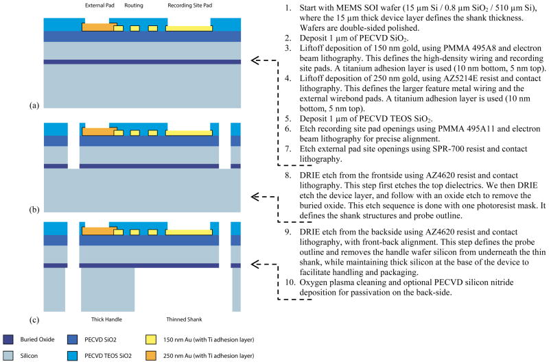
Objective: Neural recording electrodes are important tools for understanding neural codes and brain dynamics. Neural electrodes that are closely packed, such as in tetrodes, enable spatial oversampling of neural activity, which facilitates data analysis. Here we present the design and implementation of close-packed silicon microelectrodes to enable spatially oversampled recording of neural activity in a scalable fashion.

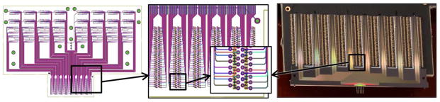
Methods: Our probes are fabricated in a hybrid lithography process, resulting in a dense array of recording sites connected to submicron dimension wiring.

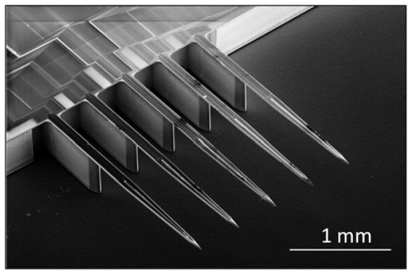
Results: We demonstrate an implementation of a probe comprising 1000 electrode pads, each 9 × 9 μm, at a pitch of 11 μm. We introduce design automation and packaging methods that allow us to readily create a large variety of different designs.

Significance: We perform neural recordings with such probes in the live mammalian brain that illustrate the spatial oversampling potential of closely packed electrode sites.


Figures

Fig. 1
Fig. 1
Close-packed recording sites on a silicon shank, for spatially oversampled neural recording. Scanning electron micrograph (SEM) of the tip of a recording shank with two columns of 100 rows each. The close-packed recording sites of 9 × 9 μm have a pitch of 11 μm, and are visible as the light squares. Insulated metal routing runs along the length of the shank, visible as dark lines flanking the rows of light squares. The shank itself has a width of ~50 μm in the region shown, and is 15 μm thick.
Fig. 2
Fig. 2
Top-down SEM view of a four-column shank of close-packed electrodes. The center columns are connected by wiring running in-between the outer pads, and all columns are then collected and routed along the two sides. The direction towards the shank tip is indicated by the arrow.
Fig. 3
Fig. 3
Simplified process cross-sections (not to scale) during key steps of the fabrication process: (a) metallization, using two different metal deposition steps, (b) front- and (c) back-side DRIE etches that define the probe shape. The shank thickness is determined by the choice of SOI device layer thickness. The process details are shown in the list on the right. The arrows indicate between which process step the cross sections correspond to. Final devices and actual cross-sections are shown in Figs. 5 and 6.
Fig. 4
Fig. 4
To route the high-density wiring from the recording sites (as shown in Fig. 1) to the large wirebond pads on the probe periphery, we use a combination of electron beam lithography (EBL) and contact (optical) lithography. The left drawing shows the 1000 channel probe’s routing scheme, from the recording sites at the very top to the wirebond pads on the bottom. EBL wiring on the probe shanks (yellow) connects to contact lithography wiring on the base of the probe (green). The center drawing shows the transitions from 8 nA to 40 nA beam currents, as well as from the 40 nA EBL to contact lithography, with the two transitions marked by dashed lines. To be able to handle alignment errors and possible wafer drift during long EBL writes, these transition regions consist of a larger landing pattern, as indicated by insets in the microscope images on the right. The white scale bars correspond to 25 μm.
Fig. 5
Fig. 5
SEM and cross section images obtained by focused ion beam (FIB), showing the metallization and recording sites. (A): an 11 μm recording site with high density wiring adjacent to it, in false color. The gold metal is shown as yellow, and comprises both the recording site and the wiring. The TEOS SiO2, shown in cyan, provides a smooth and void-free insulation layer. The silicon substrate is shown as dark blue. (B): close-up of the contact etch between two adjacent recording sites. A mild lithography misalignment of around 150 nm is noted, and the layout was designed to be indifferent against such misalignments. (C): close-up of the high density wiring where wires are 200 nm wide, placed at a 400 nm pitch, and 150 nm thick. (D): SEM of the top view of a two-column recording shank, showing the close-packed recording sites, and the wiring on the sides. The orientation of the cross sections in this figure is indicated by the dotted line. (E): a 9 μm recording site, after surface preparation by gold electroplating. False coloring used as previously in (A), but the additional electroplated gold layer (shown as orange) is visible and its surface roughness helps to lower the electrode site impedance.
Fig. 6
Fig. 6
SEM view of a 5 shank, 1000 channel probe fabricated with the process shown in Fig. 3. The 15 μm thin shanks and thicker support structures are visible. The handle wafer thickness is 510 μm, and the device layer is 15 μm. The buried oxide is 0.8 μm, sufficiently thick to serve as a DRIE etch stop during the through-wafer backside etch, but thin enough to remove easily after the frontside etch. The shanks have a pitch of 500 μm. The tip portion of one shank is shown in Fig. 1.
Fig. 7
Fig. 7
SEM view of the breakout beams that connect the side of the 1000 channel probe (right half of the image) to the bulk of the wafer (left half of the image). These beams, also visible in Fig. 8, are sufficiently strong to allow wafer handling during the last process steps without accidental breakage (unless the wafer receives a sharp shock), but weak enough to easily break with tweezers or a needle point. A wide range of beam designs are sufficient for this, but we used a U-shape bend to allow an easy access point for breaking the beams. Also visible are metal filler structures on the left, outside the probe, to facilitate the metal liftoff procedure.
Fig. 8
Fig. 8
Photographs of two wafers illustrating a large variety of designs, with probes ranging from 64 to 1000 channels. All of these devices were created automatically by parameterized cells and arranged on the wafer algorithmically. The devices in the right wafer are aligned to have the shanks point towards the wafer center, in order to avoid yield drops in the electron beam lithography that can occur close to the wafer edge. The close-up on the far right shows a section of the wafer with four 64-channel test probes. Each of these probes has different characteristics, such as the shank length or variations in recording site dimensions. A set of small breakout beams hold the otherwise released probe in place on the wafer (seen as small notches, on the bottom of the probe as well as the left and right sides on the top, identified by white arrows). Fig. 7 shows a breakout beam used in the 1000 channel design in more detail.
Fig. 9
Fig. 9
Components of the design automation: Design parameters are entered by the user in a spreadsheet, exported along with default values for any unspecified parameters, read in by a Cadence script, and automatically processed to generate all of the designs and arrange them on the wafer area.
Fig. 10
Fig. 10
Summary list (left) of the probe packaging steps, and images (center, right) of packaged probes. Electrical testing before die assembly verifies that the probe shank wiring is intact, by measuring the roundtrip resistance between two wirebond pads short-circuited at the recording sites. Center: Example of a 64-channel probe with a 5 mm long shank, held inside a plastic box for transport, using nylon threaded standoffs and thumb nuts. The PCB is assembled with the FFC connectors, and then the probe is attached and wirebonded. The photo is prior to encapsulating the probe wirebonds with an epoxy that insulates it against liquids. Right: the 1000 channel probe follows the same principle, but uses a larger PCB with 32 FFC connectors. Encapsulation was done with a clear epoxy (Loctite M-31CL).
Fig. 11
Fig. 11
PCB design schematics for the 1000-channel probe. Instead of routing the wirebonds out in a two-column bar, as done in the 64-channel probe, we break up the routing for the 1000-channel probe into a comb-shaped multi-finger design, of 8 fingers with 128 pads each (photograph of the probe after wirebonding but before encapsulation). This allows us to maintain a better aspect ratio of the silicon, and then route the wiring on the PCB across 8 inner layers to the connectors seen at the top of the schematic.
Fig. 12
Fig. 12
In vivo recordings with a close-packed electrode array in the sensory cortex of a head-fixed mouse under light (0.5%) isoflurane anesthesia. Left: example of the recorded data for a single spike across 28 pads (2 columns of 14 rows) on a 64-channel probe. Our spatial oversampling design enables the spike to be picked up by several nearby recording sites (9 × 9 μm pads, 10.5 μm pitch). The vertical scale bar is 200 μV. Right: Focusing on a single recording site (marked with a star in the probe map on the left), four consecutive spikes (top) are then overlaid (bottom) to show the spikes in more detail.
Fig. 13
Fig. 13
Electrode site characterization as a function of electrode dimensions for square pad sites. The electrode impedance into saline was measured at 1 kHz, and the magnitude of the complex impedance is shown. The probes were gold electroplated with a total charge of 11.85 μA-s/μm2, spread out across 60 pulses of 1 second duration each. As the pad size increases, the impedance drops. Even for pads as small as 3 μm × 3 μm, the electrode impedance is 2 M or less. For the 9 μm × 9 μm standard recording sites used in the closely packed probes, low impedances between 0.3 to 0.6 M are observed.
Fig. 14
Fig. 14
Electrical noise measurement as a function of electrode impedance for the same sites as shown in Fig. 13. The contribution of input referred noise from the amplifiers (2.4 μVrms) was removed from the data.

References

    1. Henze DA, et al. Intracellular Features Predicted by Extracellular Recordings in the Hippocampus In Vivo. J Neurophysiol. 2000 Jul;84(1):390–400. - PubMed
    1. Gold C, et al. On the Origin of the Extracellular Action Potential Waveform: A Modeling Study. J Neurophysiol. 2006 May;95(5):3113–3128. - PubMed
    1. Gray CM, et al. Tetrodes markedly improve the reliability and yield of multiple single-unit isolation from multi-unit recordings in cat striate cortex. J Neurosci Methods. 1995 Dec;63(1):43–54. - PubMed
    1. McNaughton BL, et al. The stereotrode: A new technique for simultaneous isolation of several single units in the central nervous system from multiple unit records. J Neurosci Methods. 1983 Aug;8(4):391–397. - PubMed
    1. Wise KD, et al. An Integrated-Circuit Approach to Extracellular Microelectrodes. IEEE Trans on Biomed Eng. 1970 Jul;17(3):238–247. - PubMed

Publication types