. 2016 Feb 1:7:10550.
doi: 10.1038/ncomms10550.

Ultra-high gain diffusion-driven organic transistor

Affiliations

Ultra-high gain diffusion-driven organic transistor

Fabrizio Torricelli et al. Nat Commun. .

Abstract

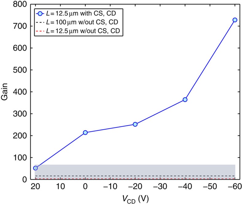
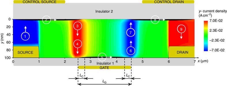
Emerging large-area technologies based on organic transistors are enabling the fabrication of low-cost flexible circuits, smart sensors and biomedical devices. High-gain transistors are essential for the development of large-scale circuit integration, high-sensitivity sensors and signal amplification in sensing systems. Unfortunately, organic field-effect transistors show limited gain, usually of the order of tens, because of the large contact resistance and channel-length modulation. Here we show a new organic field-effect transistor architecture with a gain larger than 700. This is the highest gain ever reported for organic field-effect transistors. In the proposed organic field-effect transistor, the charge injection and extraction at the metal-semiconductor contacts are driven by the charge diffusion. The ideal conditions of ohmic contacts with negligible contact resistance and flat current saturation are demonstrated. The approach is general and can be extended to any thin-film technology opening unprecedented opportunities for the development of high-performance flexible electronics.


Figures

Figure 1
Figure 1. Transistor architecture and characteristics.
(a) Top-view optical image of a diffusion-driven organic field-effect transistor (DOFET) fabricated on plastic foil OSC is the organic semiconductor. Scale bar, 5 μm. (b) DOFET components. Photolithographically patterned gold is used for metal electrodes (named gate, source, drain, control source, control drain), the insulators (insulators 1 and 2) are photoimageable polymers (polyvinylphenol), and the organic semiconductor is a solution-processed pentacene. The material thicknesses are detailed in the Supplementary Fig. 1. (c) Photograph of the plastic (PEN) foil with the measured transistors detached from the glass substrate. The transistors are fabricated with an industrial thin-film technology with three metal layers. (d,e) Measured transfer characteristics at several control source voltages. The VCS step is 10 V, VS=0 V and VCD=0 V. The DOFET channel width and length are W=100 μm and L=12.5 μm, respectively. (f) Measured output characteristics at several control drain voltages.
Figure 2
Figure 2. DOFET operation.
Two-dimensional numerical simulations. The applied voltages are VG=−5.1 V, VS=0 V, VD=−1 V, VCS=−60 V, VCD=−60 V. Geometrical and physical parameters are listed in the Supplementary Fig. 1 and in the Methods section, respectively. (a) Charge concentration in the organic semiconductor. The white arrows depict the charge injection from the source and drain electrodes into the semiconductor when the control source and control drain electrodes are biased. The x-to-y scale ratio is 1:200. (b) Quasi-Fermi potential at y=99 nm with (full line) and without (dashed line) CS/CD. Without CS/CD about half of VDS drops at the source and it is required for the charge injection. (c) Current density: x-component JX (black area) is equal to 1 A cm−2, and the y-component JY is shown with colour scale levels. (d) Current density JY and electric field EY along the y-direction at x=3.5 μm. In the range y=[0–47] nm, the current is driven by the diffusion, and in the range y=[47–100] nm, the current is driven by the drift. (e) JY and EY along the y-direction at x=20.5 μm. In the range y=[0–47] nm, the current is driven by the drift, and in the range y=[47–100] nm, the current is driven by the diffusion.
Figure 3
Figure 3. DOFET measurements and parameters.
When it is not specified, the applied voltages are: VS=0 V, VD=−1 V, VCS=0 V, VCD=0 V, and the transistors geometries are: W=100 μm, L=12.5 μm. (a) Width-normalized contact resistance RP as a function of the gate voltage VG. RP is calculated with the method. In the conventional OFET (viz. without CS and CD), RP decreases with VG, whereas in the DOFET, RP is independent of VG. When the control source is biased at VCS=+5 V, the DOFET works as a conventional coplanar OFET. (b) RP vs VCS at various VG measured on two nominally identical DOFETs. When VCS<−10 V, RP is the same for both the DOFETs and it is independent of both VG and VCS. Inset: measured output characteristics of a DOFET at several VCS. (c) Maximum overall field-effect mobility vs VCS. The inset shows the field-effect mobility as a function of the gate voltage: μFE=(L/W) (∂ID/∂VG)/(Ci VD). The × symbol is the maximum value of each curve. (d) Threshold voltage (VTH) as a function of VCS. VTH is the intercept to the VG-axis of the ID linear fit. Inset: Subthreshold slope as a function of VCS. (e) Normalized output characteristics of the DOFET measured at various VCD. ID is normalized by its maximum value at VD=−30 V. In saturation, the DOFET is an ideal current generator because the current is diffusion driven. The most important short-channel effect due to the channel-length modulation vanishes. The VCD controls the charge extraction at the drain electrode, which has a strong impact on the output conductance (gO=∂ID/∂VD). (f) Normalized output characteristics of a DOFET and two conventional OFETs (viz. without CS and CD).
Figure 4
Figure 4. 2D numerical simulations of a DOFET operating in saturation.
The applied voltages are VG=−5.1 V, VS=0 V, VD=−10 V, VCS=−60 V, VCD=−60 V. (a) Charge concentration in the organic semiconductor. (b) Current density: x-component JX (black area) is equal to 1 A cm−2, and the y-component JY is shown with colour scale levels. For the sake of clarity, the positions of control source (CS), control drain (CD) and gate electrodes are shown. Geometrical and physical parameters are listed in the Supplementary Fig. 1.
Figure 5
Figure 5. DOFET gain.
Measured gain as a function of VCD. The applied voltages are VG=−5 V, VS=0 V, VCS=−20 V. The transistors width is W=100 μm. The DOFET (full line with symbols) length is L=12.5 μm. The OFET lengths are L=12.5 μm (red dashed line) and L=100 μm (black dashed line). The other geometries are the same. The DOFET and OFET are fabricated with the same materials (Supplementary Fig. 1). The grey area shows the gain obtained in OFETs.
Figure 6
Figure 6. 2D numerical simulations of a DOFET with minimized capacitances.
Current density: x-component JX (black area) is 10 A cm−2, and the y-component JY is shown with colour scale levels. For the sake of clarity, the positions of control source (CS), control drain (CD) and gate electrodes are shown. Geometrical and physical parameters are listed in the Supplementary Fig. 1. The applied voltages are VG=−5.1 V, VS=0 V, VD=−1 V, VCS=−60 V, VCD=−60 V.

References

    1. Kaltenbrunner M. et al. An ultra-lightweight design for imperceptible plastic electronics. Nature 499, 458–463 (2013). - PubMed
    1. Nomura K. et al. Room-temperature fabrication of transparent flexible thin-film transistors using amorphous oxide semiconductors. Nature 432, 488–492 (2004). - PubMed
    1. Cao Q. et al. Medium-scale carbon nanotube thin-film integrated circuits on flexible plastic substrates. Nature 454, 495–500 (2008). - PubMed
    1. Kuribara K. et al. Organic transistors with high thermal stability for medical applications. Nat. Commun 3, 1–7 (2012). - PubMed
    1. Takei K. et al. Nanowire active-matrix circuitry for low-voltage macroscale artificial skin. Nat. Mater. 9, 821–825 (2010). - PubMed

Publication types