

Unexpected Giant-Gap Quantum Spin Hall Insulator in Chemically Decorated Plumbene Monolayer
- PMID: 26833133
- PMCID: PMC4735859
- DOI: 10.1038/srep20152
Unexpected Giant-Gap Quantum Spin Hall Insulator in Chemically Decorated Plumbene Monolayer
Abstract
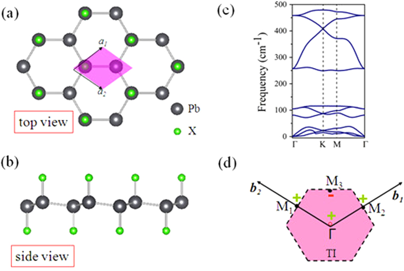
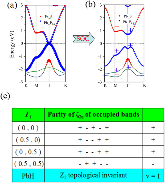
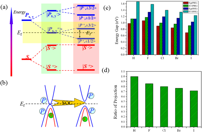
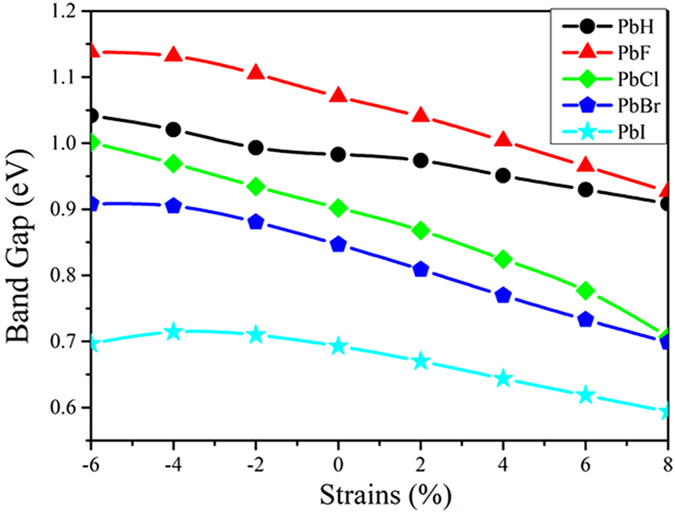
Quantum spin Hall (QSH) effect of two-dimensional (2D) materials features edge states that are topologically protected from backscattering by time-reversal symmetry. However, the major obstacles to the application for QSH effect are the lack of suitable QSH insulators with a large bulk gap. Here, we predict a novel class of 2D QSH insulators in X-decorated plumbene monolayers (PbX; X = H, F, Cl, Br, I) with extraordinarily giant bulk gaps from 1.03 eV to a record value of 1.34 eV. The topological characteristic of PbX mainly originates from s-p(x,y) band inversion related to the lattice symmetry, while the effect of spin-orbital coupling (SOC) is only to open up a giant gap. Their QSH states are identified by nontrivial topological invariant Z2 = 1, as well as a single pair of topologically protected helical edge states locating inside the bulk gap. Noticeably, the QSH gaps of PbX are tunable and robust via external strain. We also propose high-dielectric-constant BN as an ideal substrate for the experimental realization of PbX, maintaining its nontrivial topology. These novel QSH insulators with giant gaps are a promising platform to enrich topological phenomena and expand potential applications at high temperature.
Figures
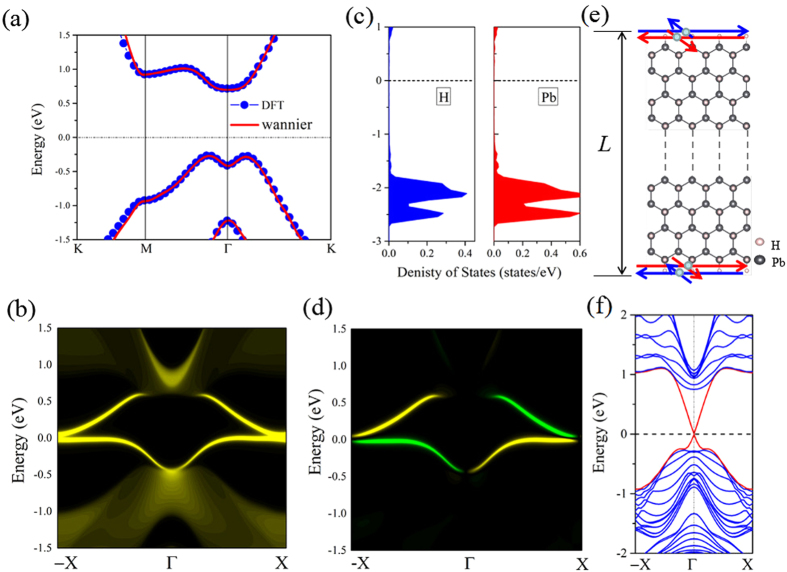
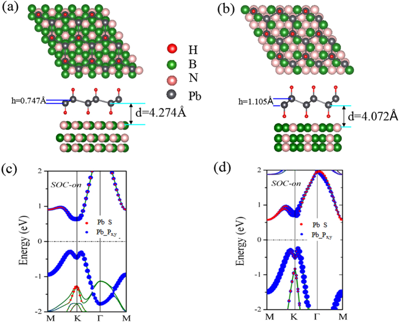
 substrate. Orbital-resolved band structures with SOC based on DFT calculations. (c,d) notes the energy band of PbH on 2 × 2 and
  BN substrate with SOC. The Fermi level is set to zero.
References
-
- Yan B. & Zhang S. C. Topological Materials. Rep. Prog. Phys. 75, 096501–096523 (2012). - PubMed
-
- Moore J. E. Majorana’s Wires. Nature nanotechnology. 8, 194–198 (2013). - PubMed
-
- Hasan M. Z. & Kane C. L. Colloquium: Topological Insulators. Rev. Mod. Phys. 82, 3045–3067 (2010).
-
- Qi X. L. & Zhang S. C. Topological Insulators and Superconductors. Rev. Mod. Phys. 83, 1057–1110 (2011).
-
- Kane C. L. & Mele E. J. Quantum Spin Hall Effect in Graphene. Phys. Rev. Lett. 95, 226801 (2005). - PubMed
Publication types
LinkOut - more resources
Full Text Sources
Other Literature Sources
Miscellaneous
