

Growing Embossed Nanostructures of Polymer Brushes on Wet-Etched Silicon Templated via Block Copolymers
- PMID: 26841692
- PMCID: PMC4740862
- DOI: 10.1038/srep20291
Growing Embossed Nanostructures of Polymer Brushes on Wet-Etched Silicon Templated via Block Copolymers
Abstract
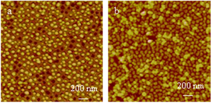
Block copolymer nanolithography has attracted enormous interest in chip technologies, such as integrated silicon chips and biochips, due to its large-scale and mass production of uniform patterns. We further modified this technology to grow embossed nanodots, nanorods, and nanofingerprints of polymer brushes on silicon from their corresponding wet-etched nanostructures covered with pendent SiHx (X = 1-3) species. Atomic force microscopy (AFM) was used to image the topomorphologies, and multiple transmission-reflection infrared spectroscopy (MTR-IR) was used to monitor the surface molecular films in each step for the sequential stepwise reactions. In addition, two layers of polymethacrylic acid (PMAA) brush nanodots were observed, which were attributed to the circumferential convergence growth and the diffusion-limited growth of the polymer brushes. The pH response of PMAA nanodots in the same region was investigated by AFM from pH 3.0 to 9.0.
Figures


Similar articles
-
Switching transport through nanopores with pH-responsive polymer brushes for controlled ion permeability.ACS Appl Mater Interfaces. 2013 Feb;5(4):1400-7. doi: 10.1021/am302820y. Epub 2013 Feb 11. ACS Appl Mater Interfaces. 2013. PMID: 23360664
-
Glucose monitoring using a polymer brush modified polypropylene hollow fiber-based hydraulic flow sensor.ACS Appl Mater Interfaces. 2015 Mar 4;7(8):4631-40. doi: 10.1021/am507927w. Epub 2015 Feb 20. ACS Appl Mater Interfaces. 2015. PMID: 25675859
-
Smart polymer brush nanostructures guide the self-assembly of pore-spanning lipid bilayers with integrated membrane proteins.Nanoscale. 2014 Feb 21;6(4):2228-37. doi: 10.1039/c3nr05356c. Epub 2014 Jan 3. Nanoscale. 2014. PMID: 24425208
-
Antibacterial surfaces based on polymer brushes: investigation on the influence of brush properties on antimicrobial peptide immobilization and antimicrobial activity.Biomacromolecules. 2011 Oct 10;12(10):3715-27. doi: 10.1021/bm2009697. Epub 2011 Sep 20. Biomacromolecules. 2011. PMID: 21902171
-
Surface Nanostructures Based on Assemblies of Polymer Brushes.Chempluschem. 2020 May;85(5):998-1007. doi: 10.1002/cplu.202000112. Epub 2020 Apr 30. Chempluschem. 2020. PMID: 32352243 Review.
Cited by
-
Bottom-up synthesis of ordered metal/oxide/metal nanodots on substrates for nanoscale resistive switching memory.Sci Rep. 2016 May 9;6:25537. doi: 10.1038/srep25537. Sci Rep. 2016. PMID: 27157385 Free PMC article.
References
-
- Bates F. S. Polymer-polymer phase behavior. Science 251, 898–905 (1991). - PubMed
-
- Whitesides G. M., Mathias J. P. & Seto C. T. Molecular self-assembly and nanochemistry: a chemical strategy for the synthesis of nanostructures. Science 254, 1312–1319 (1991). - PubMed
-
- Park M., Harrison C., Chaikin P. M., Register R. A. & Adamson D. H. Block copolymer lithography-periodic arrays of ~1011 holes in 1 square centimeter. Science 276, 1401–1404 (1997).
-
- Thurn-Albrecht T. et al. Ultrahigh-density nanowire arrays grown in self-assembled diblock copolymer templates. Science 290, 2126–2129 (2000). - PubMed
-
- Kim S. O. et al. Epitaxial self-assembly of block copolymers on lithographically defined nanopatterned substrates. Nature 424, 411–414 (2003). - PubMed
Publication types
LinkOut - more resources
Full Text Sources
Other Literature Sources
Molecular Biology Databases
Miscellaneous
