Backward spoof surface wave in plasmonic metamaterial of ultrathin metallic structure
- PMID: 26842340
- PMCID: PMC4740866
- DOI: 10.1038/srep20448
Backward spoof surface wave in plasmonic metamaterial of ultrathin metallic structure
Abstract
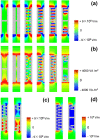
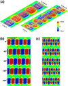
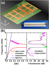
Backward wave with anti-parallel phase and group velocities is one of the basic properties associated with negative refraction and sub-diffraction image that have attracted considerable interest in the context of photonic metamaterials. It has been predicted theoretically that some plasmonic structures can also support backward wave propagation of surface plasmon polaritons (SPPs), however direct experimental demonstration has not been reported, to the best of our knowledge. In this paper, a specially designed plasmonic metamaterial of corrugated metallic strip has been proposed that can support backward spoof SPP wave propagation. The dispersion analysis, the full electromagnetic field simulation and the transmission measurement of the plasmonic metamaterial waveguide have clearly validated the backward wave propagation with dispersion relation possessing negative slope and opposite directions of group and phase velocities. As a further verification and application, a contra-directional coupler is designed and tested that can route the microwave signal to opposite terminals at different operating frequencies, indicating new application opportunities of plasmonic metamaterial in integrated functional devices and circuits for microwave and terahertz radiation.
Figures


Similar articles
-
Controlling rejections of spoof surface plasmon polaritons using metamaterial particles.Opt Express. 2014 Jun 2;22(11):13940-50. doi: 10.1364/OE.22.013940. Opt Express. 2014. PMID: 24921585
-
Trapping surface plasmon polaritons on ultrathin corrugated metallic strips in microwave frequencies.Opt Express. 2015 Mar 23;23(6):7031-7. doi: 10.1364/OE.23.007031. Opt Express. 2015. PMID: 25837047
-
High-order modes of spoof surface plasmonic wave transmission on thin metal film structure.Opt Express. 2013 Dec 16;21(25):31155-65. doi: 10.1364/OE.21.031155. Opt Express. 2013. PMID: 24514689
-
Integrated spoof plasmonic circuits.Sci Bull (Beijing). 2019 Jun 30;64(12):843-855. doi: 10.1016/j.scib.2019.01.022. Epub 2019 Feb 2. Sci Bull (Beijing). 2019. PMID: 36659674 Review.
-
Spoof surface plasmonics: principle, design, and applications.J Phys Condens Matter. 2022 Apr 28;34(26). doi: 10.1088/1361-648X/ac6558. J Phys Condens Matter. 2022. PMID: 35390773 Review.
Cited by
-
Application of confocal surface wave microscope to self-calibrated attenuation coefficient measurement by Goos-Hänchen phase shift modulation.Sci Rep. 2018 Jun 4;8(1):8547. doi: 10.1038/s41598-018-26424-2. Sci Rep. 2018. PMID: 29867205 Free PMC article.
-
Backward Phase Matching for Second Harmonic Generation in Negative-Index Conformal Surface Plasmonic Metamaterials.Adv Sci (Weinh). 2018 Aug 31;5(11):1800661. doi: 10.1002/advs.201800661. eCollection 2018 Nov. Adv Sci (Weinh). 2018. PMID: 30479919 Free PMC article.
-
Wideband helicity dependent spoof surface plasmon polaritons coupling metasurface based on dispersion design.Sci Rep. 2016 Dec 6;6:38460. doi: 10.1038/srep38460. Sci Rep. 2016. PMID: 27922132 Free PMC article.
-
Radiation loss of planar surface plasmon polaritons transmission lines at microwave frequencies.Sci Rep. 2017 Jul 21;7(1):6098. doi: 10.1038/s41598-017-06454-y. Sci Rep. 2017. PMID: 28733683 Free PMC article.
-
Isotropic Backward Waves Supported by a Spiral Array Metasurface.Sci Rep. 2018 May 8;8(1):7098. doi: 10.1038/s41598-018-25469-7. Sci Rep. 2018. PMID: 29740039 Free PMC article.
References
-
- Ramo S., Whinnery J. R. & Van Duzer T. Fields and Waves in Communication Electronics. 45–46 Wiley (1965).
-
- Veselago V. The electrodynamics of substances with simultaneously negative values of ε and μ. Soviet Physics Uspekhi 10, 509–514 (1968).
-
- Shelby R. A., Smith D. R. & Schultz S. Experimental verification of a negative index of refraction. Science 292, 77–79 (2001). - PubMed
-
- Pendry J. B. Negative refraction makes a perfect lens. Phys. Rev. Lett. 85, 3966–3969 (2000). - PubMed
-
- Fang N., Lee H., Sun C. & Zhang X. Sub-Diffraction-Limited Optical Imaging with a Silver Superlens. Science 308, 534–537 (2005). - PubMed
Publication types
LinkOut - more resources
Full Text Sources
Other Literature Sources
Research Materials
Miscellaneous

