. 2016 Mar 22;10(3):2995-3014.
doi: 10.1021/acsnano.5b03299. Epub 2016 Feb 22.

Nanomanufacturing: A Perspective

Affiliations

Nanomanufacturing: A Perspective

J Alexander Liddle et al. ACS Nano. .

Abstract

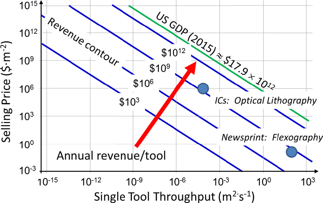
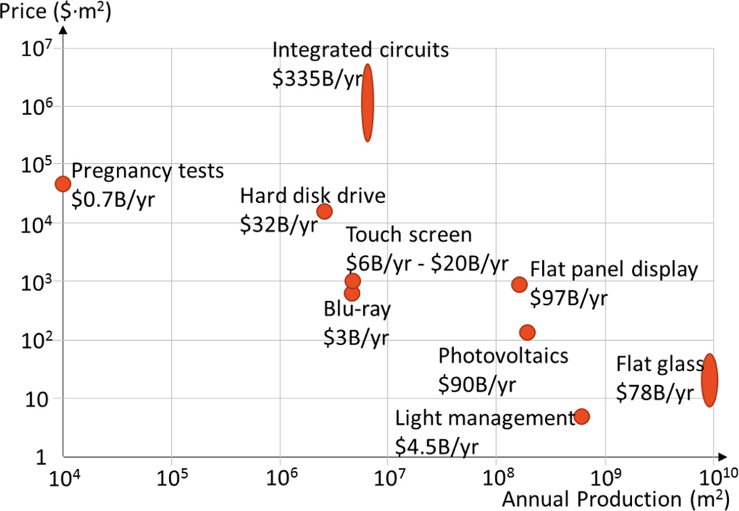
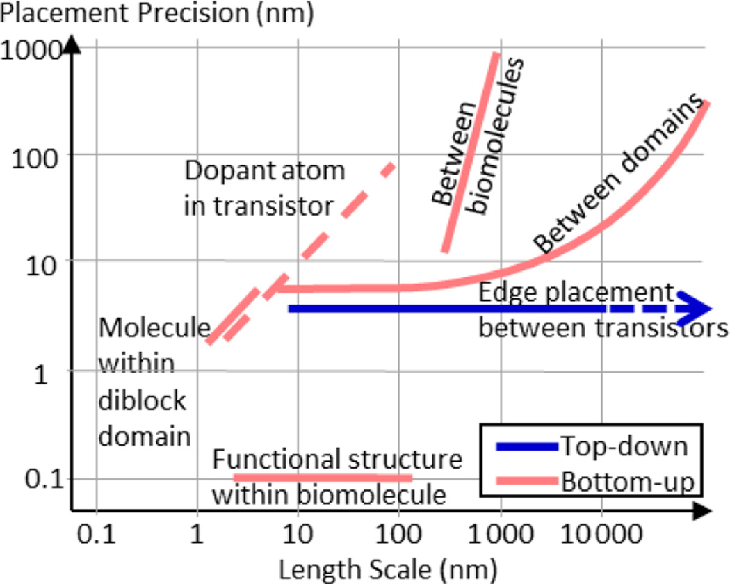
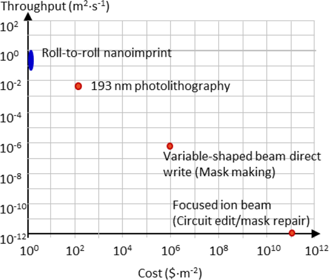
Nanomanufacturing, the commercially scalable and economically sustainable mass production of nanoscale materials and devices, represents the tangible outcome of the nanotechnology revolution. In contrast to those used in nanofabrication for research purposes, nanomanufacturing processes must satisfy the additional constraints of cost, throughput, and time to market. Taking silicon integrated circuit manufacturing as a baseline, we consider the factors involved in matching processes with products, examining the characteristics and potential of top-down and bottom-up processes, and their combination. We also discuss how a careful assessment of the way in which function can be made to follow form can enable high-volume manufacturing of nanoscale structures with the desired useful, and exciting, properties.

Keywords: lithography; nanofabrication; nanomanufacturing; self-assembly.


Figures

Figure 1
Figure 1
Log-log plot of the product selling price ($·m−2) versus single tool throughput (m2·s−1) with contours showing the relationship between throughput and selling price for different yearly revenue levels. Optical lithography as used for integrated circuit manufacturing is an example of a low-throughput process used to make a very high value product, leading to large revenues. Flexography, used for newsprint production, is a very high throughput process manufacturing a low value product, leading to more modest per-tool revenues.
Figure 2
Figure 2
Log-log plot of the approximate product selling price ($·m−2) versus global annual production (m2) for a variety of nano-enabled, or potentially nano-enabled products. Approximate market sizes (2014) are show next to each point (The SI contains the information we used to estimate each data point).
Figure 3
Figure 3
Illustration of the role of stochastic processes in controlling structural precision in top-down, bottom-up and damped-driven assembly. Placement of individual atoms, such as dopants, within semiconductor devices is effectively only as good as the device dimension, with current manufacturing methods. I.e., an atom is only constrained to lie somewhere within the “box” created. Placement of edges is typically a fraction of feature size, and is uniform within the length scale of a circuit. Systems, such as diblock copolymers, which self-assemble with no guiding pattern, show excellent short-range order that decays exponentially with distance. The placement of individual molecules within a domain is again controlled by the size of the box. i.e., the domain. Control over individual atom placement is greatest in biomolecules, where it is specified by atomic relationships in, for example, amino acids, and then by the hierarchy of secondary and tertiary structure. Placement precision between biomolecules not bound together decays rapidly as a function of separation.
Figure 4
Figure 4
Throughput (m2·s−1) versus cost ($·m−2) for top-down patterning techniques used in integrated circuit manufacturing. Despite nine orders of magnitude variation in cost and throughput, each technique falls into the nanomanufacturing, rather than nanofabrication, category in this context. While not capable of the same performance in terms of placement accuracy, roll-to-roll nanoimprint lithography is included as a point of comparison with another high-throughput nanoscale patterning technique. Note the strong negative correlation between throughput and cost.
Figure 5
Figure 5
The plot shows a measure of manufacturing complexity, MC, as a function of cost per unit area (dollars per square meter). We define manufacturing complexity (MC) as Log10 [K·ξmax/(dmin·f·P)], where K is the Kolmogorov complexity, (ξmax/dmin) is a measure of the maximum distance over which spatial coherence must be maintained, compared to the minimum feature size, the fractional tolerance, f, is the maximum allowable variation in feature size, and the perfection, P, is the maximum fraction of defective components or concentration of impurities that can be permitted. The cost may be dominated by the information content (Bits), as in the case of a Blu-ray disk, or by the material (Atoms) as for a protein-functionalized nanoparticle [see text for details].

References

    1. Martin-Palma RJ, Lakhtakia A. Nanotechnology: A Crash Course. Bellingham, WA: SPIE; 2010.
    1. Kriven WM, Lin H-T, Zhu D, Chen YL, Miller RA. Defect Clustering and Nano-Phase Structure Characterization of Multi-Component Rare Earth Oxide Doped Zirconia-Yttria Thermal Barrier Coatings. 27th Annual Cocoa Beach Conference on Advanced Ceramics and Composites: A: Ceramic Engineering and Science Proceedings. 2008;24
    1. Wang Z-y, Han E-h, Ke W. Fire-Resistant Effect of Nanoclay on Intumescent Nanocomposite Coatings. J. Appl. Polym. Sci. 2007;103:1681–1689.
    1. Salla J, Pandey KK, Srinivas K. Improvement of UV Resistance of Wood Surfaces by Using ZnO Nanoparticles. Polym. Degrad. Stab. 2012;97:592–596.
    1. Liu K, Jiang L. Bio-Inspired Self-Cleaning Surfaces. Annu. Rev. Mater. Res. 2102;42:231–263.