

Exfoliation and Raman Spectroscopic Fingerprint of Few-Layer NiPS3 Van der Waals Crystals
- PMID: 26875451
- PMCID: PMC4753463
- DOI: 10.1038/srep20904
Exfoliation and Raman Spectroscopic Fingerprint of Few-Layer NiPS3 Van der Waals Crystals
Abstract
The range of mechanically cleavable Van der Waals crystals covers materials with diverse physical and chemical properties. However, very few of these materials exhibit magnetism or magnetic order, and thus the provision of cleavable magnetic compounds would supply invaluable building blocks for the design of heterostructures assembled from Van der Waals crystals. Here we report the first successful isolation of monolayer and few-layer samples of the compound nickel phosphorus trisulfide (NiPS3) by mechanical exfoliation. This material belongs to the class of transition metal phosphorus trisulfides (MPS3), several of which exhibit antiferromagnetic order at low temperature, and which have not been reported in the form of ultrathin sheets so far. We establish layer numbers by optical bright field microscopy and atomic force microscopy, and perform a detailed Raman spectroscopic characterization of bilayer and thicker NiPS3 flakes. Raman spectral features are strong functions of excitation wavelength and sample thickness, highlighting the important role of interlayer coupling. Furthermore, our observations provide a spectral fingerprint for distinct layer numbers, allowing us to establish a sensitive and convenient means for layer number determination.
Figures
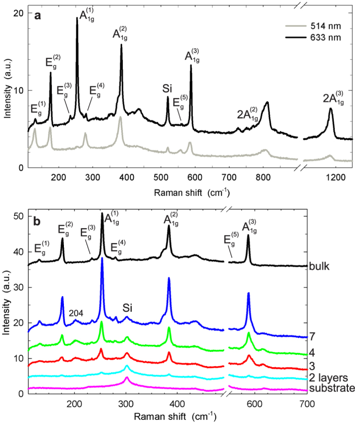
 nm), acquired at excitation wavelengths
  and 633 nm. These spectra are indistinguishable from those reported for bulk NiPS3. 5 in-plane
  and 3 out-of-plane
  phonon modes are indicated. The Raman peak of silicon visible at 520 cm−1 stems from the substrate. (b) Spectra of thin NiPS3 sheets (2–7 layers), acquired at
  nm, together with the spectrum of a thick sheet shown in panel (a), and the substrate spectrum. All spectra were acquired in a single pass, under identical experimental conditions, on the sample shown in Fig. 1d. Spectra have not been scaled; data are offset vertically for clarity. The spectral region dominated by the first-order Raman peak of the silicon substrate around 520 cm−1 has been omitted. The spectral feature at ~300 cm−1 is a second-order Raman peak of silicon.
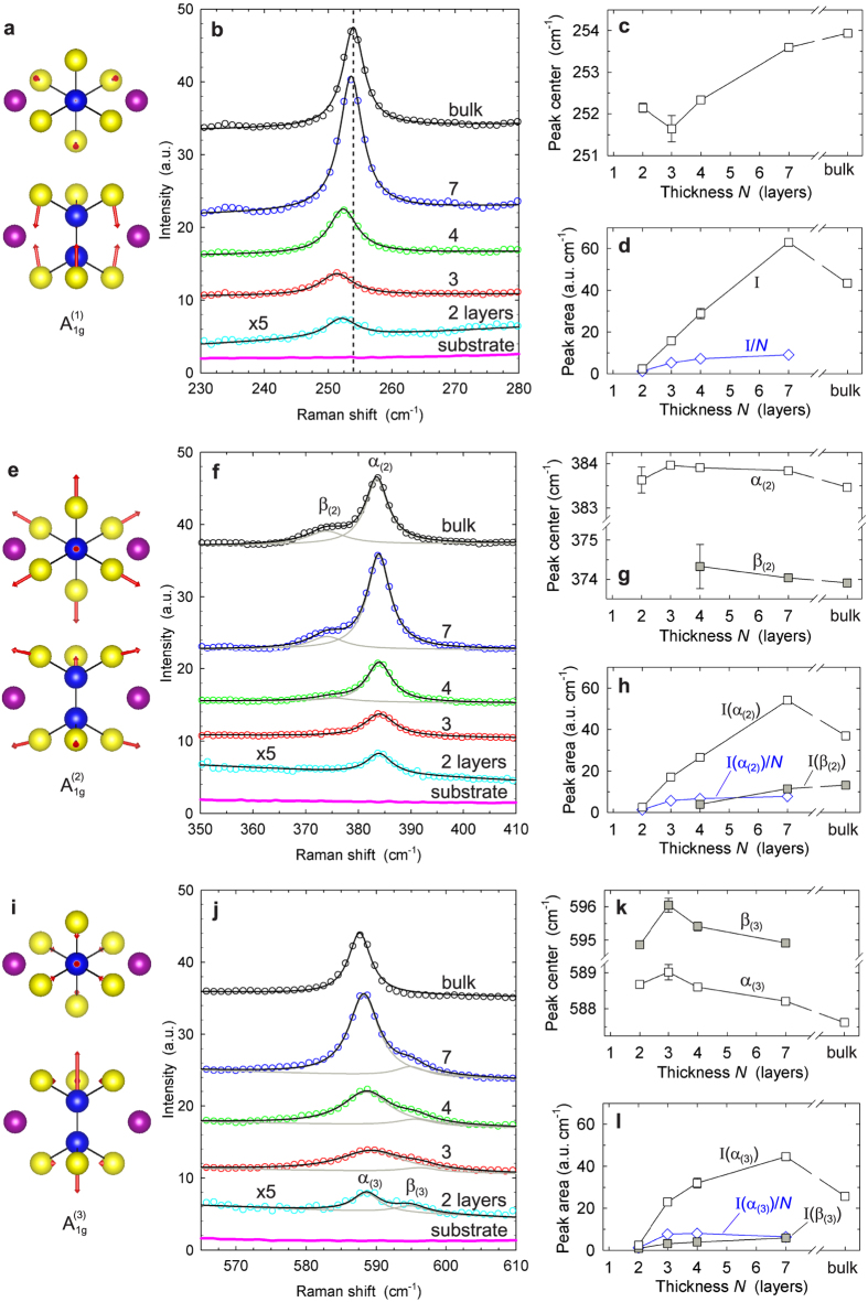
 phonon mode. (b) Detailed view of Raman data in corresponding spectral range, for thin sheets (2–7 layers), thick sheet, and silicon substrate. Spectra are overlayed with Lorentzian line shape fits. Data of bilayer sample have been magnified by factor 5. Spectra are offset vertically for clarity. (c) Central frequencies determined by Lorentzian peak fits in (b). Error bars correspond to spread of experimental data. (d) Integrated line shape intensities
  (=peak area) determined by Lorentzian peak fits in (b). (e–h) Analogous information for
  phonon mode. Raman spectra of 4-layer, 7-layer and thick NiPS3 sheets are composed of two distinct Lorentzian lines: individual Lorentzian fit curves (grey lines) and sum of fit curves (black lines). (i–l) Analogous information for
  phonon mode. Raman spectra of thin sheets (2–7 layers) contain two superimposed Lorentzian lines.
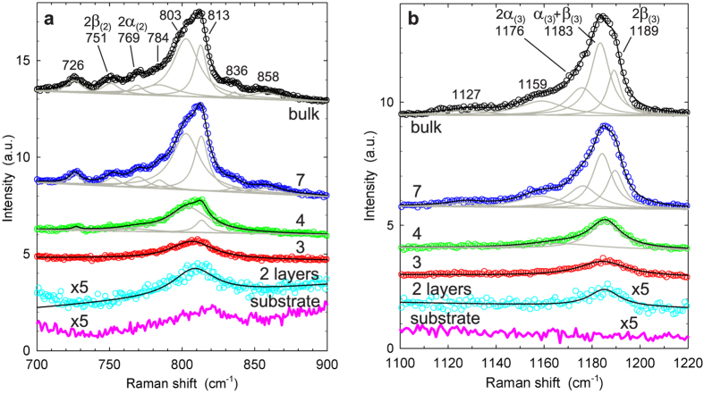
 second-order processes. Spectra are described by superposition of up to 8 Lorentzian peak shapes: individual Lorentzian fit curves (grey lines) and sum of fit curves (black lines). Labels state wavelength shifts (in cm−1) of individual peak centers. Data of bilayer sample and substrate have been magnified by factor 5. Spectra are offset vertically for clarity. (b) Spectral range containing
  second-order processes. Spectra are described by up to 5 Lorentzian line shapes. See the text for details.
References
-
- Novoselov K. S. et al. Electric Field Effect in Atomically Thin Carbon Films. Science 306, 666–669 (2004). - PubMed
-
- Castro Neto A. H., Guinea F., Peres N. M. R., Novoselov K. S. & Geim A. K. The Electronic Properties of Graphene. Rev. Mod. Phys. 81, 109–162 (2009).
-
- Schedin F. et al. Detection of Individual Gas Molecules Adsorbed on Graphene. Nat. Mater. 6, 652–655 (2007). - PubMed
-
- Chen J.-H., Jang C., Xiao S., Ishigami M. & Fuhrer M. S. Intrinsic and Extrinsic Performance Limits of Graphene Devices on SiO2. Nat. Nanotechnol. 3, 206–209 (2008). - PubMed
-
- Dean C. R. et al. Boron Nitride Substrates for High-Quality Graphene Electronics. Nat. Nanotechnol. 5, 722–726 (2010). - PubMed
Publication types
LinkOut - more resources
Full Text Sources
Other Literature Sources
