. 2016 Feb 18:6:21650.
doi: 10.1038/srep21650.

Deep-UV nitride-on-silicon microdisk lasers

Affiliations

Deep-UV nitride-on-silicon microdisk lasers

J Sellés et al. Sci Rep. .

Abstract

Deep ultra-violet semiconductor lasers have numerous applications for optical storage and biochemistry. Many strategies based on nitride heterostructures and adapted substrates have been investigated to develop efficient active layers in this spectral range, starting with AlGaN quantum wells on AlN substrates and more recently sapphire and SiC substrates. Here we report an efficient and simple solution relying on binary GaN/AlN quantum wells grown on a thin AlN buffer layer on a silicon substrate. This active region is embedded in microdisk photonic resonators of high quality factors and allows the demonstration of a deep ultra-violet microlaser operating at 275 nm at room temperature under optical pumping, with a spontaneous emission coupling factor β = (4 ± 2) 10(-4). The ability of the active layer to be released from the silicon substrate and to be grown on silicon-on-insulator substrates opens the way to future developments of nitride nanophotonic platforms on silicon.


Figures

Figure 1
Figure 1. Structural properties of the nitride-on-silicon microdisks.
(a) Schematic view of a microdisk. The structure is composed of an AlN disk with twenty GaN/AlN quantum wells (0.7 nm quantum well – 5 nm barrier), maintained by a silicon post on a silicon substrate; the distribution of the electric field intensity of a WGM is illustrated on the top of the disk, as calculated for a TE mode in a 2 μm-diameter microdisk (radial order n = 1, azimutal order m = 33, vertical confinement number q = 1). As indicated by arrows, the microdisk is excited at normal incidence by the pump laser and the emission is collected from the edge. (b) Transmission Electron Micrograph (TEM) of the GaN/AlN quantum wells. (c) Scanning Electron Micrograph (SEM) of a 8 μm-diameter microdisk. (d) Atomic Force Micrograph of the AlN buffer layer.
Figure 2
Figure 2. Room temperature lasing of a 3 μm-diameter microdisk.
(a) Emission spectra under pulsed excitation taken at different pump powers (spectra are shifted for clarity). The spectral resolution is 0.17 meV. (b) PL spectrum of the same microdisk under continuous wave excitation, compared to the one of the un-processed active layer (excitation power density: 500 W.cm−2, same spectral resolution). The values of quality factors for some WGMs are indicated. (c) Integrated intensity (filled circles) and linewidth (empty squares) measured for lasing peak A1. The linewidth uncertainty is due to the slight irreversible energy shifts observed along the acquisitions at low excitation power, and carrier-induced or temperature-induced effects at high excitation power. The β-factor of the A1 mode is fitted by the rate equation model described in Supplementary Note 2 (plain blue line).
Figure 3
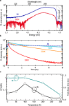
Figure 3. Optical properties of the active layer.
(a) Photoluminescence of the active region at 5 K (full blue line) and 300 K (full red line). The QWs are excited by 200 fs pulses at 4.66 eV/266 nm. The grey dashed area represents the cutoff of the filter discriminating the photoluminescence from the scattered laser. (b) Time-resolved photoluminescence recorded at 5 K (blue line) and its bi-exponential decay fit (white dashed line). Experimental data at 100 K (cyan line), 200 K (orange line) and 300 K (red line) are also represented. (c) Integrated PL intensity normalized at T = 5 K (blue squares) and fast decay time (black dots) versus temperature.
Figure 4
Figure 4. Microdisk laser emission versus disk diameter.
Photoluminescence spectra taken above threshold for a wide range of microdisk diameters. Spectra are shifted for clarity. The top spectrum corresponds to a nitride microdisk directly lying on oxide following growth on a SOI substrate and underetching, and the other ones to nitride microdisks standing on a Si post. The spectrometer resolution is 1 meV. Inset: Average spectra (dots) of 20 investigated microdisks standing on a Si post (all diameters), recorded above lasing threshold at P/Pthr = 1.3. The red line is a guide for the eye.

References

    1. Nanishi Y. Nobel Prize in Physics: The birth of the blue LED. Nat. Photonics 10.1038/nphoton.2014.291 (2014) - DOI
    1. Amano H., Kito M., Hiramatsu K. & Akasaki I. P-Type Conduction in Mg-Doped GaN Treated with Low-Energy Electron Beam Irradiation (LEEBI). Jpn. J. Appl. Phys. 28, L2112–L2114 (1989).
    1. Nakamura S., Mukai T. & Senoh M. High-Power GaN P-N Junction Blue-Light-Emitting Diodes. Jpn. J. Appl. Phys. 30, L1998–L2001 (1991).
    1. Pust P. et al. Narrow-band red-emitting Sr[LiAl3N4]:Eu2+ as a next-generation LED-phosphor material. Nat. Mater 13, 891–896 (2014). - PubMed
    1. Taniyasu Y., Kasu M. & Makimoto T. An aluminium nitride light-emitting diode with a wavelength of 210 nanometres. Nature 441, 325–328 (2006). - PubMed

Publication types

LinkOut - more resources