Topologically nontrivial bismuth(111) thin films
- PMID: 26888122
- PMCID: PMC4758034
- DOI: 10.1038/srep21326
Topologically nontrivial bismuth(111) thin films
Abstract
Using high-resolution angle-resolved photoemission spectroscopy (ARPES), the topological property of the three-dimensional Bi(111) films grown on the Bi2Te3(111) substrate were studied. Very different from the bulk Bi, we found another surface band near the point besides the two well-known surface bands on the 30 nm films. With this new surface band, the bulk valence band and the bulk conduction band can be connected by the surface states in the Bi(111)/Bi2Te3 films. Our band mapping revealed odd number of Fermi crossings of the surface bands, which provided new experimental evidences that Bi(111)/Bi2Te3 films of a certain thickness can be topologically nontrivial in three dimension.
Figures

 is poor.

 -
- -
- near
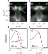
near  point. The incident photon energy hν = 30 eV. Green dash lines mark bulk valence band. (c) Black and red lines are EDCs of 30nm Bi at
  point and of Au. An energy gap was observed. (d) Black and and red lines are EDCs of 20 nm Bi at
  point and of Au. There is no energy gap.
 point along
  -
- -
- (incident photon energy hν = 42, 46, 44, 40, 38 and 36 eV). Green and blue dashed lines are the guides for the S1, S2 and S3 bands. (g) MDCs near Fermi level extracted from (a). Greed dotted lines mark MDC peaks of S1. (h) SDI plot of ARPES spectra (hν = 30 eV) near
  point along
  -
- -
- direction. Green dashed line shows the possible dispersion of S1 band. (i) High resolution EDCs along
  -
- (hν = 30 eV). Green and blue dotted lines mark EDC peaks of S1 and S3 bands. (j) The corresponding ARPES spectra of (i). (k) Four EDCs from (j). The momentum positions are indicted by the red lines in (j) (k = 0.43 \AA−1, 0.56 \AA−1, 0.60 \AA−1, 0.70 \AA−1). (l) EDCs at
  point as a function of the incident photon energy.
References
-
- Bernevig B. A., Hughes T. L. & Zhang S. C. Quantum spin Hall effect and topological phase transition in HgTe quantum wells. Science 314, 1757–1761 (2006). - PubMed
-
- König M. et al. Quantum spin Hall insulator state in HgTe quantum wells. Science 318, 766–770 (2007). - PubMed
-
- Fu L. & Kane C. L. Topological insulators with inversion symmetry. Phys. Rev. B 76, 045302 (2007).
-
- Hsieh D. et al. A topological Dirac insulator in a quantum spin Hall phase. Nature 452, 970–974 (2008). - PubMed
-
- Zhang H. et al. Topological insulators in Bi2Se3, Bi2Te3 and Sb2Te3 with a single Dirac cone on the surface. Nat. Phys. 5, 438–442 (2009).
Publication types
LinkOut - more resources
Full Text Sources
Other Literature Sources

