. 2015 Jun;8(6):3024-3052.
doi: 10.3390/ma8063024. Epub 2015 May 28.

Review of Recent Progress of Plasmonic Materials and Nano-Structures for Surface-Enhanced Raman Scattering

Affiliations

Review of Recent Progress of Plasmonic Materials and Nano-Structures for Surface-Enhanced Raman Scattering

Alan X Wang et al. Materials (Basel). 2015 Jun.

Abstract

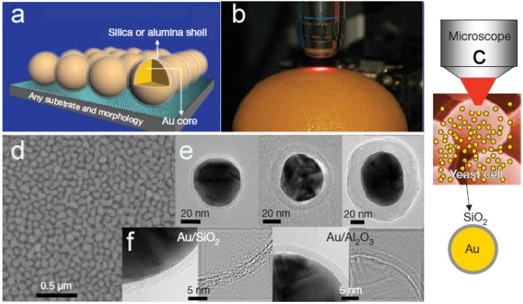
Surface-enhanced Raman scattering (SERS) has demonstrated single-molecule sensitivity and is becoming intensively investigated due to its significant potential in chemical and biomedical applications. SERS sensing is highly dependent on the substrate, where excitation of the localized surface plasmons (LSPs) enhances the Raman scattering signals of proximate analyte molecules. This paper reviews research progress of SERS substrates based on both plasmonic materials and nano-photonic structures. We first discuss basic plasmonic materials, such as metallic nanoparticles and nano-rods prepared by conventional bottom-up chemical synthesis processes. Then, we review rationally-designed plasmonic nano-structures created by top-down approaches or fine-controlled synthesis with high-density hot-spots to provide large SERS enhancement factors (EFs). Finally, we discuss the research progress of hybrid SERS substrates through the integration of plasmonic nano-structures with other nano-photonic devices, such as photonic crystals, bio-enabled nanomaterials, guided-wave systems, micro-fluidics and graphene.

Keywords: optical sensors; photonic crystals; plasmonic materials; surface plasmons; surface-enhanced Raman scattering.


Figures

Figure 1
Figure 1
Schematic illustration of the fabrication process of a surface-enhanced Raman scattering (SERS) biosensor for protein recognition. AuNPs with a diameter of around 13 nm labeled with antibody and the Raman probe molecule were used as immuno-gold colloids, which were crosslinked onto the solid chip during the process of immunoassay detection. After the Ag colloids’ deposition, the SERS signal of the Raman probe was obtained [56]. (Reproduced with permission from Wang et al., published by Royal Society of Chemistry, 2007.)
Figure 2
Figure 2
(a) The working principles of the shell-isolated nanoparticle-enhanced Raman spectroscopy (SHINERS) mode; (b) in situ inspection of pesticide residues on fruit by SHINERS; (c) in situ probing of biological structures by SHINERS; (d) SEM image of a monolayer of Au/SiO2 nanoparticles on a smooth Au surface; (e) HRTEM images of Au/SiO2 core-shell nanoparticles with different shell thicknesses; (f) HRTEM images of Au/SiO2 nanoparticle and Au/Al2O3 nanoparticle with a continuous and completely packed shell about 2 nm thick [67]. (Reproduced with permission from Li et al., published by Nature Publishing Group, 2010.)
Figure 3
Figure 3
Photographs of Langmuir–Blodgett (LB) nanowire assembly process (a,b) at different compression stages. SEM images (c,d) of the Ag nanowire monolayer deposited on a silicon wafer at different magnifications [75]. (Reproduced with permission from Tao et al., published by ACS, 2003.)
Figure 4
Figure 4
Representative metallic nanomaterials with different geometric morphologies: (A) SEM images of Ag nanoprisms [89] (reproduced with permission from Yang et al., published by John Wiley and Sons, 2014); (B) SEM images of Ag nanocubes [90] (reproduced with permission from Sun et al., published by AAAS, 2002); (C) TEM images of Au nanostars [94] (reproduced with permission from Yuan et al., published by ACS, 2012); (D) SEM images of Ag nanosheets [96] (reproduced with permission from Yan et al., published by ACS, 2012).
Figure 5
Figure 5
Schematic illustration of a colloidal crystal mask (A) and representative AFM image (B) of Ag nano-triangular structures. Ambient contact mode atomic force microscope image of 200-nm Ag over 542-nm diameter polystyrene spheres: (C) array of spheres (10 μm × 10 μm) and (D) image (600 nm × 600 nm) of one sphere showing substructure roughness with schematic illustration [97,101]. (Reproduced with permission from Van Duyne et al., published by ACS 2001, 2002.)
Figure 6
Figure 6
(A) SEM images of on-wire lithography (OWL)-generated nanodisk arrays with various geometries; (B) Confocal Raman microscopy images of gapped nanowire structures functionalized with methylene blue (MB) [104]. (Reproduced with permission from Qin et al., published by National Academy of Sciences, USA, 2006.)
Figure 7
Figure 7
(A) (Top) Structure of a tri-layer nanocapsule; (bottom) with the electric tweezers, nanocapsules can be transported and assembled onto a pre-patterned array of nanomagnets by utilizing the magnetic attraction force between the Ni segments in the nanocapsules and the magnetic layers inside the nanomagnets [108] (reproduced with permission from Xu et al., published by John Wiley and Sons, 2012); (B) SEM images of silica nanotubes embedded with Ni nanomagnets and a close view of the AgNPs on the nanotube surface [109] (reproduced with permission from Xu et al., published by John Wiley and Sons, 2013); (C) Raman mapping profile of 1 μM Rhodamine 6G dispersed on a tri-layer nanocapsule shows uniform SERS intensity on the entire surface of the nanocapsules. (1655 cm−1, scan step 250 nm, integration time 0.5 s) [109] (reproduced with permission from Xu et al., published by John Wiley and Sons, 2013); (D) Electric tweezers using AC and DC configurations on quadruple electrodes for the manipulation of nanocapsules [108] (reproduced with permission from Xu et al., published by John Wiley and Sons, 2012).
Figure 8
Figure 8
(A) Electro-migrated gaps from [122] (reproduced with permission from Ward et al., published by ACS, 2007). (B) Helium ion microscope image (45°) and schematic diagram of multiphoton-lithography SERS substrate (left). Hot-spot isolation (HSI) process (right): (1) diluted positive-tone photoresist is spin-coated onto a SERS substrate to cover the surface; (2) a femtosecond laser pulse train is scanned over the surface, selectively exposing the photoresist covering electromagnetic hot-spots; (3) the photoresist is developed, and the SERS hot-spots are uncovered [123] (reproduced with permission from Diebold et al., published by ACS 2009). (C) (Left) Schematic illustrations of the preparation of preclosed and 1,2-bi-(4-pyridyl) ethylene (BPE)-trapped gold fingers. The inset shows the magnified view of finger tips. (Right) SEM images of as-fabricated and closed fingers [127] (reproduced with permission from Kim et al., published by ACS, 2011).
Figure 9
Figure 9
(A) (Top) The geometry of the dielectric grating structure with silver nanorod optical antennas on 2D silicon nitride grating surface. (Bottom right) Field map |E|/|E0| at the surface of the grating at resonance. (Bottom left) |E|/|E0| versus wavelength calculated by rigorous coupled wave analysis (RCWA) at Point A as marked on the inset to the right. |E0| is the magnitude of the incident electric field [138] (reproduced with permission from Li et al., published by American Institute of Physics, 2009). (B) Schematic diagram of PC-SERS substrate of SiO2-Ag “post-cap” nanostructure with a thickness of the SiO2 layer of 75 nm and a thickness of the Ag layer of 20 nm by the oblique angle deposition method [139] (reproduced with permission from Kim et al., published by Optical Society of America, 2010). (C) Measured 1 µM R6G Raman spectrum from the plasmonic nanotube on the flat Si3N4 substrate and from the plasmonic nanotube on the GMR grating. The inset figures show the SEM image of the grating and the optical image of the plasmonic nanotube on top of the grating [41] (reproduced with permission from Xu et al., published by American Institute of Physics, 2012).
Figure 10
Figure 10
(A) SEM images of various diatom species with different frustules [141] (reproduced with permission). (B) SEM image of the hybrid diatom-plasmonic SERS substrates [151] (reproduced with permission from Yang et al., published by John Wiley and Sons, 2014). (C) The 1 μM R6G Raman mapping results from the hybrid diatom-plasmonic SERS substrate [150] (reproduced with permission from Ren et al., published by IEEE, 2014). (D) Schematic diagram of the diatom-plasmonic SERS immunoassay using a standard antigen-antibody model.
Figure 11
Figure 11
(A) Fiber-optic SERS sensors through the incorporation of alumina nanoparticles and silver coatings onto the single mode fiber probe tip [154] (reproduced with permission from Stokes et al., published by Elsevier, 2000). (B) Schematic depiction of the configuration used to characterize the SERS fiber optic probe and a scanning electron micrograph of an array of gold optical antennas on the facet of a fiber [155]. (Reproduced with permission from Smythe et al., published by ACS, 2009).

References

    1. Fleischmann M., Hendra P.J., McQuillan A. Raman Spectra of Pyridine Adsorbed at a Silver Electrode. Chem. Phys. Lett. 1974;26:163–166. doi: 10.1016/0009-2614(74)85388-1. - DOI
    1. Jeanmaire D.L., van Duyne R.P. Surface raman spectroelectrochemistry: Part I. Heterocyclic, aromatic, and aliphatic amines adsorbed on the anodized silver electrode. J. Electroanal. Chem. Interfacial Electrochem. 1977;84:1–20. doi: 10.1016/S0022-0728(77)80224-6. - DOI
    1. Albrecht M.G., Creighton J.A. Anomalously Intense Raman Spectra of Pyridine at a Silver Electrode. J. Am. Chem. Soc. 1977;99:5215–5217. doi: 10.1021/ja00457a071. - DOI
    1. Tian Z. Surface-Enhanced Raman Spectroscopy: Advancements and Applications. J. Raman Spectrosc. 2005;36:466–470. doi: 10.1002/jrs.1378. - DOI
    1. Qian X., Nie S. Single-Molecule and Single-Nanoparticle SERS: From Fundamental Mechanisms to Biomedical Applications. Chem. Soc. Rev. 2008;37:912–920. doi: 10.1039/b708839f. - DOI - PubMed