

Dependence of lattice strain relaxation, absorbance, and sheet resistance on thickness in textured ZnO@B transparent conductive oxide for thin-film solar cell applications
- PMID: 26925355
- PMCID: PMC4734349
- DOI: 10.3762/bjnano.7.9
Dependence of lattice strain relaxation, absorbance, and sheet resistance on thickness in textured ZnO@B transparent conductive oxide for thin-film solar cell applications
Abstract
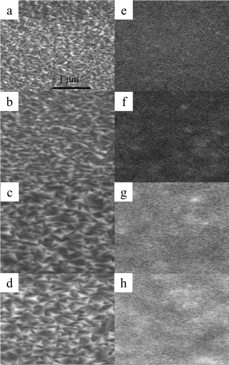
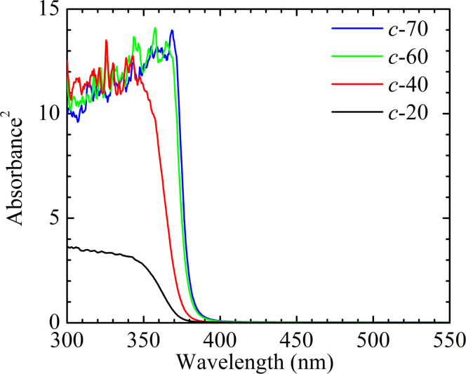
The interplay of surface texture, strain relaxation, absorbance, grain size, and sheet resistance in textured, boron-doped ZnO (ZnO@B), transparent conductive oxide (TCO) materials of different thicknesses used for thin film, solar cell applications is investigated. The residual strain induced by the lattice mismatch and the difference in the thermal expansion coefficient for thicker ZnO@B is relaxed, leading to an increased surface texture, stronger absorbance, larger grain size, and lower sheet resistance. These experimental results reveal the optical and material characteristics of the TCO layer, which could be useful for enhancing the performance of solar cells through an optimized TCO layer.
Keywords: absorbance; low-pressure chemical vapor deposition; strain relaxation; textured ZnO; transparent conductive oxide.
Figures


References
-
- Morkoç H, Özgür Ü. Zinc Oxide: Fundamentals, Materials and Device Technology. Weinheim, Germany: Wiley-VCH; 2007. - DOI
-
- Özgür Ü, Alivov Ya I, Liu C, Teke A, Reshchikov M A, Doğan S, Avrutin V, Cho S J, Morkoç H. J Appl Phys. 2005;98:041301. doi: 10.1063/1.1992666. - DOI
-
- Lai C M, Huang Y E, Kou K Y, Chen C H, Tu L W, Feng S W. Appl Phys Lett. 2015;107:022110. doi: 10.1063/1.4926978. - DOI
-
- Söderström T, Dominé D, Feltrin A, Despeisse M, Meillaud F, Bugnon G, Boccard M, Cuony P, Haug F J, Faÿ S, et al. Proc SPIE. 2010;7603:76030B. doi: 10.1117/12.843511. - DOI
-
- Chen X L, Liu J M, Ni J, Zhao Y, Zhang X D. Appl Surf Sci. 2015;328:193–197. doi: 10.1016/j.apsusc.2014.12.018. - DOI
LinkOut - more resources
Full Text Sources
Other Literature Sources