. 2016 Mar 29:7:11137.
doi: 10.1038/ncomms11137.

Microelectromechanical reprogrammable logic device

Affiliations

Microelectromechanical reprogrammable logic device

M A A Hafiz et al. Nat Commun. .

Abstract

In modern computing, the Boolean logic operations are set by interconnect schemes between the transistors. As the miniaturization in the component level to enhance the computational power is rapidly approaching physical limits, alternative computing methods are vigorously pursued. One of the desired aspects in the future computing approaches is the provision for hardware reconfigurability at run time to allow enhanced functionality. Here we demonstrate a reprogrammable logic device based on the electrothermal frequency modulation scheme of a single microelectromechanical resonator, capable of performing all the fundamental 2-bit logic functions as well as n-bit logic operations. Logic functions are performed by actively tuning the linear resonance frequency of the resonator operated at room temperature and under modest vacuum conditions, reprogrammable by the a.c.-driving frequency. The device is fabricated using complementary metal oxide semiconductor compatible mass fabrication process, suitable for on-chip integration, and promises an alternative electromechanical computing scheme.


Figures
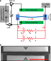
Figure 1
Figure 1. Clamped–clamped arch resonator.
(a) Schematic of the arch beam resonator and the two-port electrical transmission measurement configuration together with a parasitic current compensation circuitry using single-to-differential driver (AD8131) and a variable compensation capacitor, Ccomp. The drive electrode is provided with an a.c. signal from one of the outputs from AD8131 and the beam electrode is biased with a d.c. voltage source. The output current induced at the sense-electrode is coupled with the compensation capacitor and followed by a low-noise amplifier (LNA) whose output is coupled to the network analyser input port. Two voltage sources, VA and VB and switches, A and B are connected in parallel across the beam to perform logic operations by electrothermal tuning of the resonance frequency. The arrow in the red represents the current flowing through the beam, responsible for electrothermal frequency modulation. (b) An SEM image of the microbeam resonator. Scale bar, 200 μm.
Figure 2
Figure 2. Electrical circuit configuration of the logic input conditions.
(a) The electrical circuit represents the (0,0) logic input condition where the total current IT through the beam RMB is zero. (b) The circuit represents the (0,1) logic input condition corresponds to switch A, OFF and switch B, ON where the total current IT flowing through the beam RMB is IB. (c) The circuit represents the (1,0) logic input condition corresponds to switch A, ON and switch B, OFF where the total current IT flowing through the beam RMB is IA. (d) The circuit represents the (1,1) logic input condition corresponds to switch A, ON and switch B, ON where the total current IT flowing through the beam RMB is IA+IB.
Figure 3
Figure 3. Electrothermal frequency modulation.
Frequency responses of the resonator for different logic input conditions, (0,0), (0,1), (1,0) and (1,1), shown in black, red, blue and green, respectively.
Figure 4
Figure 4. Demonstration of 2-bit NOR and OR logic gates.
(a) Frequency responses of the resonator for different logic input conditions where (0,0) logic input condition, shown in black has high S21 transmission signal at 117.663 kHz and others have low S21 transmission signal represented by 1 and 0, respectively. Truth table of NOR logic output is shown in the inset. (b) Demonstration of NOR logic operation when the frequency of the a.c. input signal is chosen as 117.663 kHz. Two input signals A and B are shown in black and red, respectively, where the switch OFF/ON corresponds to 0/1 logic input conditions. The S21 transmission signal in blue corresponds to the logic output and fulfills the NOR truth table. (c) Frequency responses of the resonator for different logic input conditions, where (0,0) logic input condition shown in black has low S21 transmission signal at 117.361 kHz and others have high S21 transmission signal, represented by 0 and 1, respectively. Truth table for OR logic output shown in the inset. (d) Demonstration of OR logic operation when the a.c. input signal frequency is chosen as 117.361 kHz. Two input signals, A and B are shown in black and red, respectively, and the switch OFF/ON corresponds to 0/1 logic input conditions. The S21 transmission signal in blue corresponds to the logic output that fulfills the OR truth table.
Figure 5
Figure 5. Demonstration of NOT gate.
(a) Frequency responses of the resonator for different logic input conditions, where (0,0) logic input condition shown in black has high S21 transmission signal at 117.663 kHz and others have low S21 transmission signal represented by 1 and 0, respectively. Truth table of NOT logic gate is shown in the inset. (b) Demonstration of NOT logic operation when the frequency of the a.c. input signal is chosen as 117.663 kHz. Two input signals, A and B are shown in black and red, respectively, where the switch OFF/ON corresponds to 0/1 logic input conditions. S21 transmission signal in blue corresponds to the logic output and fulfills the NOT truth table.
Figure 6
Figure 6. Demonstration of 2-bit XOR and XNOR logic gates.
(a) Frequency responses of the resonator for different logic input conditions, where (0,1) and (1,0) logic input condition shown in red and blue has high S21 transmission signal at 121.43 kHz and others have low S21 transmission signal represented by 1 and 0, respectively. Truth table of XOR logic gate is shown in the inset. (b) Demonstration of XOR logic operation when the operation frequency is chosen as 121.43 kHz. Two input signals, A and B are shown in black and red, respectively, where the switch OFF/ON corresponds to 0/1 logic input conditions. S21 transmission signal in blue corresponds to the logic output that fulfills the XOR truth table. (c) Frequency responses of the resonator for different logic input conditions, where (0,0) and (1,1) logic input conditions shown in red and blue, respectively, has low S21 transmission signal at 121.281 kHz and others have high S21 transmission signal represented by 0 and 1, respectively. Truth table of XNOR logic output is shown in the inset. (d) Demonstration of XNOR logic operation when the operating frequency is fixed at 121.281 kHz. Two input signals, A and B are shown in black and red, respectively, where the switch OFF/ON corresponds to 0/1 logic input conditions. S21 transmission signal in blue corresponds to the logic output and fulfills the XNOR truth table.
Figure 7
Figure 7. Demonstration of 2-bit AND and NAND logic gates.
(a) Frequency responses of the resonator for different logic input conditions, where (1,1) logic input condition shown in magenta has high S21 transmission signal at 128.969 kHz and others have low signal represented by 1 and 0, respectively. Truth table of AND logic output is shown in the inset. (b) Demonstration of AND logic operation when the operation of frequency is chosen as 128.969 kHz. Two input signals, A and B are shown in black and red, respectively, where the switch OFF/ON corresponds to 0/1 logic input conditions. S21 transmission signal in blue corresponds to the logic output and fulfills the AND truth table. (c) Frequency responses of the resonator for different logic input conditions, where (1,1) logic input condition has low S21 transmission signal at 128.819 kHz and others have high S21 transmission signal represented by 0 and 1, respectively. Truth table of NAND logic output is shown in the inset. (d) Demonstration of NAND logic operation when the operation of frequency is chosen as 128.819 kHz. Two input signals, A and B are shown in black and red, respectively, where the switch OFF/ON corresponds to 0/1 logic input conditions. S21 transmission signal in blue corresponds to the logic output and fulfills the NAND truth table.
Figure 8
Figure 8. Realization of 3-bit logic gates.
Frequency responses of the resonator for three different input logic conditions. NOR gate is realized by choosing the frequency of operation at 119.022 kHz, where (0,0,0) logic input condition has high S21 transmission signal and all the others have low S21 transmission signal. By choosing the corresponding anti resonance dip frequency, 3-bit OR gate can be realized. A 3-bit AND gate is realized by choosing the frequency of operation at 132.105 kHz, where (1,1,1) logic input condition has high S21 transmission signal and all others have low S21 transmission signal. By choosing the corresponding anti resonance dip frequency, a 3-bit NAND gate can be realized.
Figure 9
Figure 9. Demonstration of 3-bit logic gates.
(a) Demonstration of 3-bit NOR logic operation when the operating frequency is chosen at 119.022 kHz. Three input signals, A, B, and C are shown in black, red, and blue, respectively, where the switch OFF/ON corresponds to 0/1 logic input conditions. S21 transmission signal in green corresponds to the logic output and fulfills the NOR truth table. (b) Demonstration of 3-bit AND logic operation when the operation frequency is chosen at 132.105 kHz. Three input signals, A, B, and C are shown in black, red, and blue, respectively, where the switch OFF/ON corresponds to 0/1 logic input conditions. S21 transmission signal in green corresponds to the logic output and fulfills the AND truth table.

References

    1. Babbage H. P. Babbage's Calculating Engines Vol. 2, The MIT Press (1984).
    1. Davis M. The Universal Computer Norton (2000).
    1. Theis T. N. & Horn P. M. Basic research in the information technology industry. Phys. Today 56, 44–49 (2003).
    1. Swade D. D. Redeeming Charles Babbage's mechanical computer. Sci. Am. 268, 86–91 (1993). - PubMed
    1. Halg B. On a micro-electro-mechanical nonvolatile memory cell. IEEE Trans. Electron Devices 37, 2230–2236 (1990).

Publication types