. 2016 Apr 12;113(15):3938-43.
doi: 10.1073/pnas.1504451113. Epub 2016 Mar 24.

Modulation of nitrogen vacancy charge state and fluorescence in nanodiamonds using electrochemical potential

Affiliations

Modulation of nitrogen vacancy charge state and fluorescence in nanodiamonds using electrochemical potential

Sinan Karaveli et al. Proc Natl Acad Sci U S A. .

Abstract

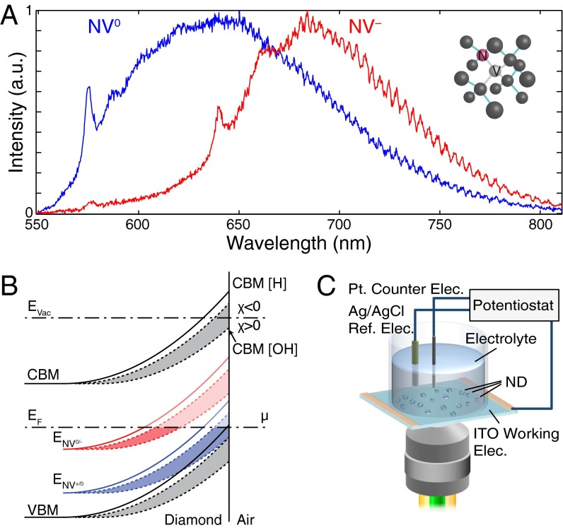
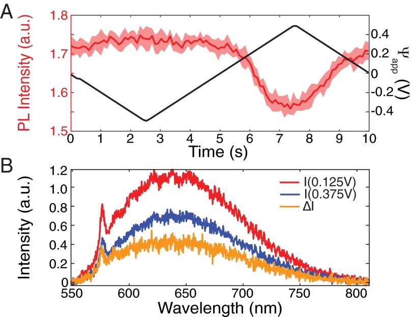
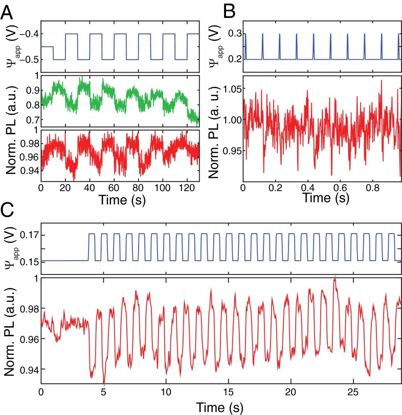
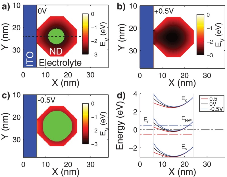
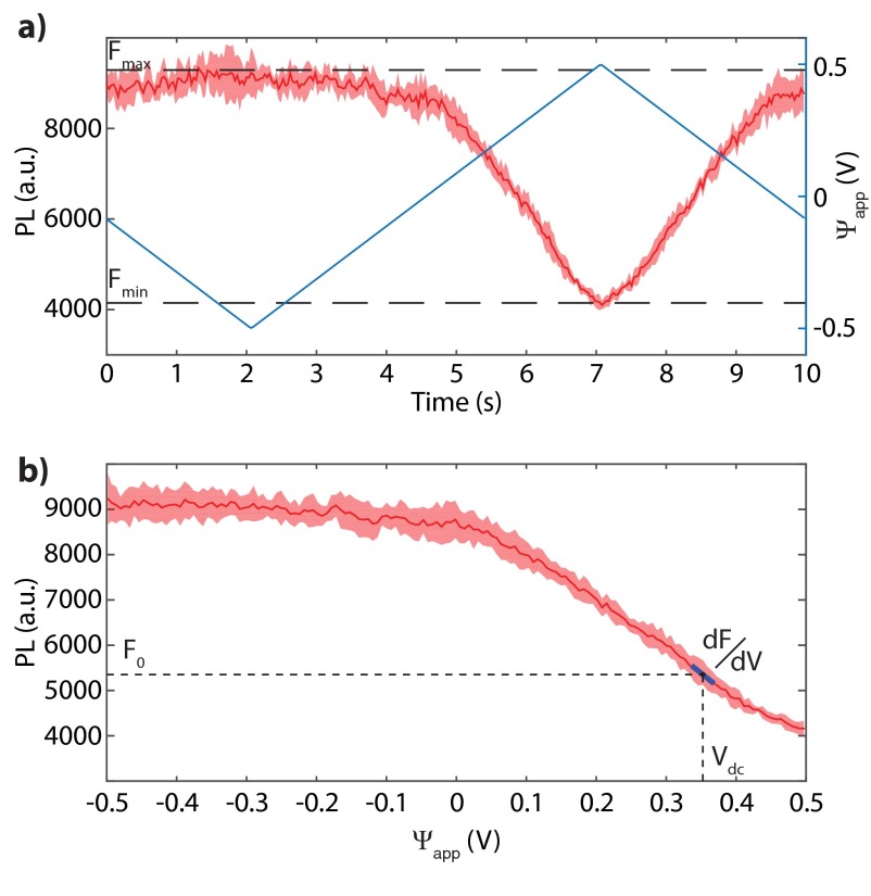
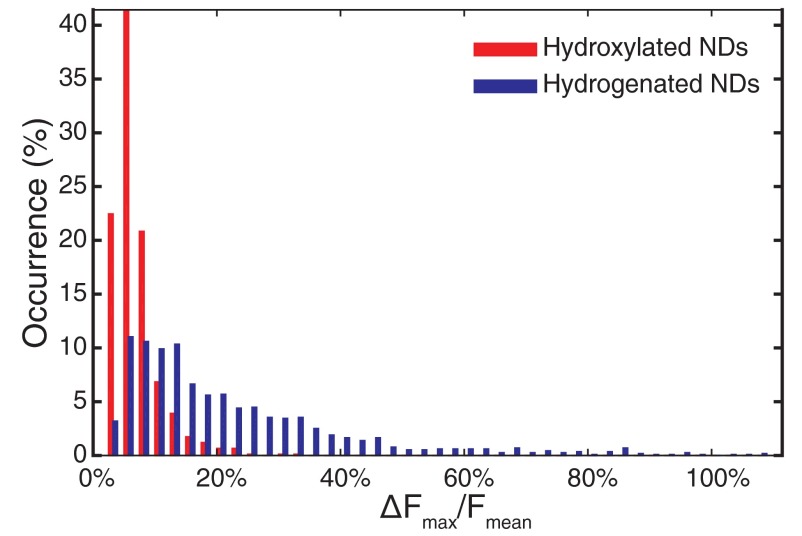
The negatively charged nitrogen vacancy (NV(-)) center in diamond has attracted strong interest for a wide range of sensing and quantum information processing applications. To this end, recent work has focused on controlling the NV charge state, whose stability strongly depends on its electrostatic environment. Here, we demonstrate that the charge state and fluorescence dynamics of single NV centers in nanodiamonds with different surface terminations can be controlled by an externally applied potential difference in an electrochemical cell. The voltage dependence of the NV charge state can be used to stabilize the NV(-) state for spin-based sensing protocols and provides a method of charge state-dependent fluorescence sensing of electrochemical potentials. We detect clear NV fluorescence modulation for voltage changes down to 100 mV, with a single NV and down to 20 mV with multiple NV centers in a wide-field imaging mode. These results suggest that NV centers in nanodiamonds could enable parallel optical detection of biologically relevant electrochemical potentials.

Keywords: fluorescence microscopy; nanodiamond; nitrogen vacancy center; voltage indicator; voltage sensing.


Conflict of interest statement

The authors declare no conflict of interest.

Figures

Fig. 1.
Fig. 1.
NV fluorescence and experimental setup schematic. (A) Fluorescence emission spectra of neutrally (blue) and negatively (red) charged NV centers in HPHT NDs. (Inset) Illustration of the NV center in the diamond lattice. (B) Energy band structure schematic showing the band bending near hydrogen (solid) and hydroxyl (dashed) terminated diamond surfaces in atmospheric conditions. Schematic of the energy band structure and near surface band bending for hydrogen (H) and hyhdroxyl (OH) surface terminated diamond in atmospheric conditions. Hydrogen surface termination results in a strongly negative electron affinity, whereas hydroxyl (OH) surface termination can have a range of both positive or negative electron affinity depending on the crystallographic orientation of diamond (gray shaded region). Equilibration of the Fermi level (EF) with the redox couple of a surface adsorbate layer induces the band bending, shifting the conduction (CBM), and valence (VBM) bands together with the NV charge state transition levels ENV0/− (red) and ENV+/0 (blue). Close to the surface, these transition levels can move above EF (light red and blue lines) and result in a change in the NV charge state depending on their distance to the surface. (C) Schematic of the electrochemical setup used to apply voltages while monitoring the ND fluorescence.
Fig. 2.
Fig. 2.
Wide-field fluorescence measurement results of hydroxylated NDs. (A) Typical wide-field fluorescence image of hydroxylated NDs on the ITO working electrode. (B) Fluorescence time traces of three different spots under repetitive triangular voltage sweep extracted from wide-field measurements. (Right) Average fluorescence (solid lines) and its SD (shaded region) for the eight voltage cycles. (C) Distribution of the maximum PL change (ΔFmax) normalized to the SD of PL (Fstd) for each measured fluorescent spot. Of the ∼4,300 different fluorescent spots, 21% showed PL modulation larger than 1.5 Fstd. (D) Statistical distribution of hydroxylated nanodiamond NV PL modulation due to the applied potential difference. PL modulation is categorized into eight types of voltage responses. The majority (93.8%) of the NV centers exhibit increased PL at negative voltages and decreased PL at positive voltages, corresponding to modulation types 1–3.
Fig. 3.
Fig. 3.
Voltage-dependent fluorescence of a single NV center in a hydroxylated ND. (A) Cycle-averaged mean PL response to applied potential difference, obtained from the wide-field data similar to Fig. 2B, for an isolated single NV center. (B) PL spectrum of the same NV center obtained at 0 V (blue) and at −0.75 V (red). The difference between the two spectra (orange shaded region) indicates that the NV portion of the spectrum increases.
Fig. 4.
Fig. 4.
Wide-field fluorescence measurement results of hydrogenated NDs. (A) Typical wide-field fluorescence image of hydrogenated NDs on the ITO. (B) Fluorescence time traces of the different clusters of NDs indicated in A under repetitive triangular voltage sweep acquired with a 562 LP filter. (Right) Average fluorescence (solid lines) and its SD (shaded region) for the eight voltage cycles. (C) Distribution of the maximum PL change (ΔFmax) normalized to the SD of PL (Fstd) for each measured fluorescent spot. Of the ∼1,200 different NV NDs, 89% showed PL modulation larger than 1.5 Fstd. (D) Statistical distribution of hydrogenated ND NV PL modulation due to the applied potential difference. PL modulation is categorized into eight types of voltage responses. Among the ones that exhibited voltage dependence, almost all (>98%) show increased PL at negative voltages and decreased PL at positive voltages, corresponding to modulation types 1–3.
Fig. 5.
Fig. 5.
Voltage-dependent fluorescence of a single NV center in a hydrogenated ND. (A) Cycle-averaged mean PL response to applied potential difference, obtained from the wide-field data similar to Fig. 4B, for an isolated single NV center. (B) PL spectrum of the same NV center obtained by applying a 250-mV amplitude square-wave voltage with a DC bias of 125 and 375 mV, corresponding to an average Ψapp of 0.125 (blue) and 0.375 V (red), respectively. Both spectra show purely NV0 fluorescence, with the difference between the two showing that the PL change is due to a decrease in NV0 fluorescence.
Fig. 6.
Fig. 6.
Detection of small voltage variations. (A) PL time traces of two isolated hydroxylated NDs to 100-mV voltage changes. (B) PL time trace of a hydrogenated ND cluster to 5-ms, 100-mV square voltage pulses. (C) PL time trace of multiple ND clusters to 20-mV voltage changes.
Fig. S1.
Fig. S1.
Numerical simulation result of the energy band diagram of the ITO/nanodiamond/electrolyte system. 2D map of the valence band maxima for (A) 0, (B) +0.5, and (C) −0.5 V. The regions for which ENV0/− < EF are highlighted in green. (D) Energy band diagram of the cross-section highlighted in A for the three applied potential differences.
Fig. S2.
Fig. S2.
FTIR spectra of (A) the hydroxylated nanodiamonds and (B) hydrogenated nanodiamonds. (A) (O-H)ν modes on the diamond surface are observed at 2,700–3,500 cm−1 due to adsorbed water, whereas the (O-H)δ can be seen at 1,640 cm−1. The (C = O)ν mode at 1,780 cm−1 and (C-O)ν at 1,100 cm−1 is still observed due to acids and alcohols. (B) (C-H)ν modes on the ND surface are observed at 2,800–2,900 cm−1, whereas the (C-H)δ can be seen at 1,360–1,500 cm−1. The (C-O)ν mode at 1,100 cm−1 is still observed due to alcohols, whereas a sharp mode at 1,260 cm−1 is believed to be (C = C)ν.
Fig. S3.
Fig. S3.
(A) Histograms of the diameters of the two types of HPHT NDs used in this study. The histograms were generated from size measurements of TEM images taken from each sample. The hydrogenated NDs have size of 12 ± 5 nm and the hydroxylated NDs have a size of 18 ± 8 nm, based on a 100 ND ensemble. The size was estimated from the TEM analysis with a spherical particle shape model as described in the procedure. (B) A representative TEM image.
Fig. S4.
Fig. S4.
(A) Fluorescence time trace measurements for the same NV center for a rectangular voltage signal acquired with a fiber-based confocal HBT setup. (B) Second-order autocorrelation result obtained from the analysis of photon arrival times at two different Ψapp values shown in A.
Fig. S5.
Fig. S5.
Fitting of the PL spectra at 0 (A) and −0.75 V (B) to the linear combination of NV0 and NV reference spectra shown in Fig. 1.
Fig. S6.
Fig. S6.
Single NV in hydrogenated nanodiamond lifetime analysis. Applied potential difference (A) and corresponding PL time traces (B) of a single NV center as determined from second-order autocorrelation measurements (C). PL decay traces (D) at 0 (red) and 0.5 V (blue) together with the instrument response function (IRF) and the fits to decay traces (dashed lines).
Fig. S7.
Fig. S7.
Example cycle-averaged PL data as a function of time (A) and as function Ψapp (B).
Fig. S8.
Fig. S8.
Statistical distribution of the modulation depth for each fluorescent spot for hydroxylated (red) and hydrogenated (blue) ND samples.
Fig. S9.
Fig. S9.
Analysis of the distribution of the DC bias voltages for (A) hydroxylated and (B) hydrogenated NDs, together with the average dF/dV normalized to F0 at each DC bias voltage value.
Fig. S10.
Fig. S10.
Distribution of the maximum PL change (ΔFmax) normalized to the SD of PL (Fstd) for each measured fluorescent spot in (A) hydroxylated and (B) hydrogenated NDs on 5 nm Al2O3-coated ITO electrodes. (A) For hydroxylated NDs, 13% of 222 measured fluorescent spots showed PL change larger than 1.5 Fstd. (B) For hydrogenated NDs, 1.2% of 728 measured fluorescent spots showed PL change larger than 1.5 Fstd.

Similar articles

Cited by

References

    1. Tamarat P, et al. Stark shift control of single optical centers in diamond. Phys Rev Lett. 2006;97(8):083002. - PubMed
    1. Bassett LC, Heremans FJ, Yale CG, Buckley BB, Awschalom DD. Electrical tuning of single nitrogen-vacancy center optical transitions enhanced by photoinduced fields. Phys Rev Lett. 2011;107(26):266403. - PubMed
    1. Dolde F, et al. Electric-field sensing using single diamond spins. Nat Phys. 2011;7(6):459–463.
    1. Maze JR, et al. Nanoscale magnetic sensing with an individual electronic spin in diamond. Nature. 2008;455(7213):644–647. - PubMed
    1. Gaebel T, et al. Photochromism in single nitrogen-vacancy defect in diamond. Appl Phys B. 2006;82(2):243–246.

Publication types