. 2016 Apr 20:6:24771.
doi: 10.1038/srep24771.

Fast Flexible Transistors with a Nanotrench Structure

Affiliations

Fast Flexible Transistors with a Nanotrench Structure

Jung-Hun Seo et al. Sci Rep. .

Abstract

The simplification of fabrication processes that can define very fine patterns for large-area flexible radio-frequency (RF) applications is very desirable because it is generally very challenging to realize submicron scale patterns on flexible substrates. Conventional nanoscale patterning methods, such as e-beam lithography, cannot be easily applied to such applications. On the other hand, recent advances in nanoimprinting lithography (NIL) may enable the fabrication of large-area nanoelectronics, especially flexible RF electronics with finely defined patterns, thereby significantly broadening RF applications. Here we report a generic strategy for fabricating high-performance flexible Si nanomembrane (NM)-based RF thin-film transistors (TFTs), capable of over 100 GHz operation in theory, with NIL patterned deep-submicron-scale channel lengths. A unique 3-dimensional etched-trench-channel configuration was used to allow for TFT fabrication compatible with flexible substrates. Optimal device parameters were obtained through device simulation to understand the underlying device physics and to enhance device controllability. Experimentally, a record-breaking 38 GHz maximum oscillation frequency fmax value has been successfully demonstrated from TFTs with a 2 μm gate length built with flexible Si NM on plastic substrates.


Figures

Figure 1
Figure 1
Comparison of the device structures (cross-sectional view) and fabrication processes between (a) 3-D nano trench Si NM flexible RF TFTs, and (b) conventional 2-D TFTs. The effective channel lengths Lch are marked in red in (a3,b3). The smallest Lch of the nano trench TFT can reach down to 50 nm via NIL and that of the conventional TFT can only reach down to about 1.5 μm. (a1) Blanket phosphorous ion implantation and thermal anneal. (a2) Nano trench formation via nanoimprint. (a3) Final structure of nano trench TFT where the channel length Lch is defined by nanoimprint. (b1) Photolithography to define S/D regions for ion implantation. (b2) Selective ion implantation and thermal anneal. (b3) Final structure of conventional TFT where the channel length Lch is limited by gate electrode and dopant out-diffusion during ion implantation and thermal anneal.
Figure 2
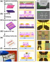
Figure 2. Fabrication process for nano trench Si NM flexible RF TFTs by NIL.
Schematic illustration (left column), cross section structure (middle column), and corresponding microscopic images (right column) of nano trench Si NM flexible RF TFTs. (a) Defining a nano trench on a phosphorus implanted p− SOI substrate using NIL. (b) Dry etching to separate the n+ area in order to form a path of n+/p−/n+ from source to drain. (c) A partially completed TFT after undercutting the buried oxide to release the Si NM, which forms the active region, and forming the source and drain contacts. (d) Flip transfer of the Si NM with the source and drain electrodes onto an adhesive coated PET substrate. (e) Dry etching to define the perimeter of the active region. (f) Deposition of an Al2O3 gate dielectric layers and gold gate electrodes above the trench. (g) Optical image of arrays of the bent TFTs on a PET substrate.
Figure 3
Figure 3. Simulated current density near the channel region for different depths and widths of the trench.
The total thickness of the Si NM (p− layer plus n+ layer) is 270 nm. The thickness of the n+ layer is 180 nm and that of the p− layer thickness is 90 nm. For all the scenarios simulated, the metal gate length (Lg) remains at 4 μm. (a) The trench width/channel length (Lch) is fixed at 100 nm. (a)(i) Simulated current density for a TFT with a 200 nm deep trench (20 nm of the trench depth extends into the p− layer: 70 nm p− layer remains as the active channel) revealing that the majority of the current flows through the trench surface and field-effect controllability is weak. (ii) At 220 nm deep (40 nm of the trench depth extends into the p− layer: 50 nm p− layer remains as the active channel), which is the middle value of the depth between the n+/p− interface and the top surface of Si NM, gate controllability is improved but a leakage current is still present through the trench. (iii) Simulated current density with the 250 nm deep trench (70 nm of the trench depth extends into the p− layer: 20 nm p− layer remains as the active channel) forms a very strong field-effected channel without a leakage current. (b) Dependence on the trench depth reduces as the width of the trench (Lch) becomes wider. The trench depth (D) is fixed at 200 nm. (i) The 100 nm wide and 200 nm deep trench shows a large leakage current near the trench surface. (ii) The 200 nm wide (Lch) trench significantly reduces the leakage current. (iii) The 500 nm wide (Lch) trench is completely free from the leakage current.
Figure 4
Figure 4. DC characteristics of the TFTs with various trench gaps/channel lengths (Lch).
Drain current versus drain voltage, Id − Vds, output curves are shown. All devices have 2 μm of gate length (Lg) and biased with Vgs ranging from 0 V to 1.5 V with a 0.3 V step (a) Devices with a 100 nm gap and a channel width and length of 20 μm and 100 nm. (b) Devices with a 200 nm gap and a channel width and length of 20 μm and 200 nm. (c) Devices with a 500 nm gap and a channel width and length of 20 μm and 500 nm. (d) Merged drain current versus gate voltage, Id − Vgs, transfer curves and transconductance (gm) with Vds = 0.1 V for these three devices. The two arrows show the directions of reducing Lch. (e) i) A microscope image of a bent array of TFTs and ring oscillators on a PET substrate. ii) A microscopic image of a single 5-stage ring oscillator under a flat condition. (f) Measured voltage–time characteristic of the 5-stage ring oscillator showing a fosc of 165 MHz and a td of 0.59 nsec.
Figure 5
Figure 5. Measured (solid lines) and simulated (dashed lines) RF characteristics of the trench TFTs with various trench gaps/channel lengths (Lch).
The gate length (Lg) in all TFTs is 2 μm. Current gain (H21) and power gain (Gmax) as a function of the frequency of a Si NM TFT with a (a) 100 nm, (b) 200 nm, and (c) 500 nm wide trench (Lch). (d,e) fT and fmax as a function of gate bias under a fixed drain bias (Vds = 1.5 V) and as a function of drain bias under a fixed gate bias (Vg = 0.6 V for 100 nm and 200 nm TFTs and Vg = 1.2 V for 500 nm TFTs). (f,g) fT and fmax as a function of bending induced external strain. (h) The small-signal equivalent circuit model used for TFT parameters extraction. (i) Image of bending setup for RF measurements.

References

    1. Kim S. et al. Low‐Power Flexible Organic Light‐Emitting Diode Display Device. Adv. Mater. 23, 3511–3516 (2011). - PubMed
    1. Kim D.-H. et al. Epidermal Electronics. Science 333(6044), 838–843 (2011). - PubMed
    1. Fan Z. et al. Three-dimensional nanopillar-array photovoltaics on low-cost and flexible substrates, Nat. Mater. 8, 648–653 (2009). - PubMed
    1. Rojas J. P., Sevilla G. A. T. & Hussain M. M. Can We Build a Truly High Performance Computer Which is Flexible and Transparent? Sci. Rep. 3, 2609 (2013). - PMC - PubMed
    1. Sirringhaus H. et al. High-resolution inkjet printing of all-polymer transistor circuits. Science 290, 2123–2126 (2000). - PubMed

Publication types

LinkOut - more resources