

Disordered array of Au covered Silicon nanowires for SERS biosensing combined with electrochemical detection
- PMID: 27112197
- PMCID: PMC4844982
- DOI: 10.1038/srep25099
Disordered array of Au covered Silicon nanowires for SERS biosensing combined with electrochemical detection
Abstract
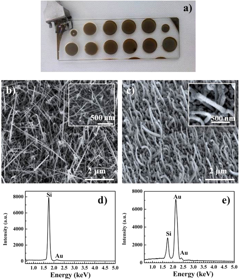
We report on highly disordered array of Au coated silicon nanowires (Au/SiNWs) as surface enhanced Raman scattering (SERS) probe combined with electrochemical detection for biosensing applications. SiNWs, few microns long, were grown by plasma enhanced chemical vapor deposition on common microscope slides and covered by Au evaporated film, 150 nm thick. The capability of the resulting composite structure to act as SERS biosensor was studied via the biotin-avidin interaction: the Raman signal obtained from this structure allowed to follow each surface modification step as well as to detect efficiently avidin molecules over a broad range of concentrations from micromolar down to the nanomolar values. The metallic coverage wrapping SiNWs was exploited also to obtain a dual detection of the same bioanalyte by electrochemical impedance spectroscopy (EIS). Indeed, the SERS signal and impedance modifications induced by the biomolecule perturbations on the metalized surface of the NWs were monitored on the very same three-electrode device with the Au/SiNWs acting as both working electrode and SERS probe.
Figures
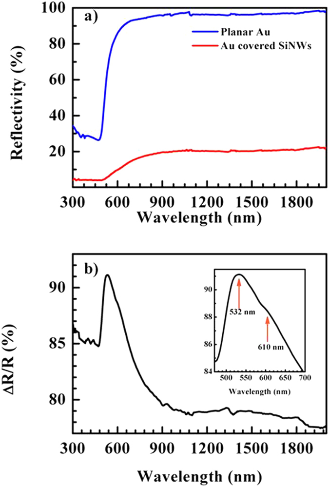
 , where RAu and RAu/SiNW are the reflectivity of the planar Au and the Au/SiNWs, respectively (b). In the inset the enlarged
  at smaller wavelengths.
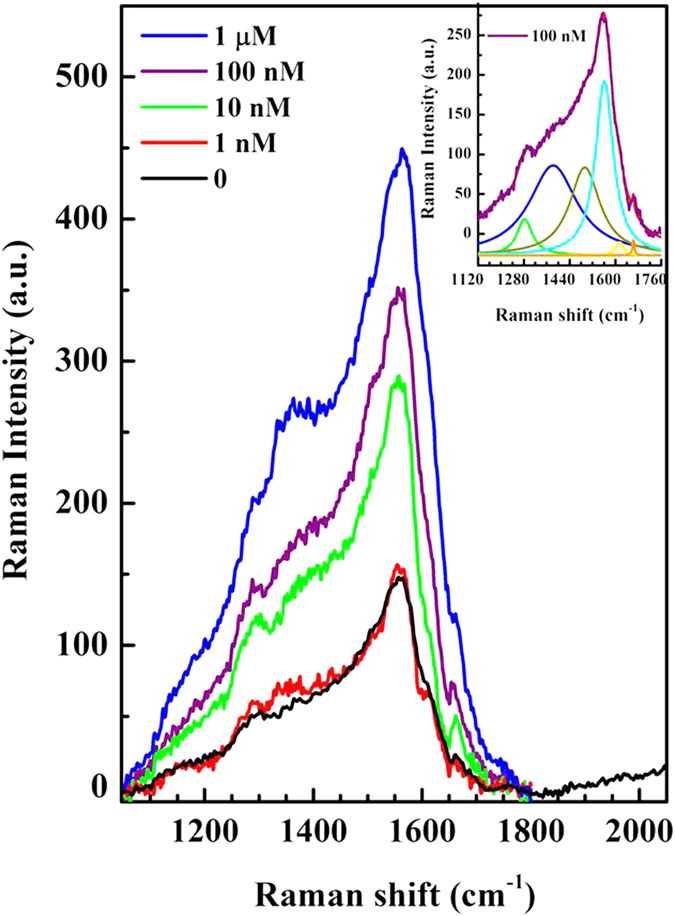
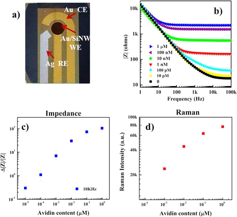
 , on the avidin concentration obtained at the frequency of 10 KHz. The values correspond to the average measurements performed on a minimum of three samples, identically treated. The relative standard deviation is indicated by the error bars (c). Intensity of the Raman band at about 1380 cm−1 ascribed to the binding of avidin on the biosensor surface, tuned as for the impedance measurements. The reported values represent the band area obtained by means of a fitting procedure applied to the collected spectra (d).
References
-
- Sharma B., Frontiera R. R., Henry A. I., Ringe E. & Van Duyne R. P. SERS: Materials, applications, and the future. Materials Today 15, 16–25 (2012).
-
- Fateixa S., Nogueira H. I. S. & Trindad T. Hybrid nanostructures for SERS: materials development and chemical detection. Phys. Chem. Chem. Phys. 17, 21046–21071 (2015). - PubMed
-
- Hakonen A., Andersson P. O., Schmidt M. S., Rindzevicius T. & Käll M. Explosive and chemical threat detection by surface-enhanced Raman scattering: A review. Analytica Chimica Acta 893, 1–13 (2015). - PubMed
-
- Kneipp K., Kneipp H., Itzkan I., Dasari R. R. & Feld M. S. Surface-enhanced Raman scattering and biophysics. J. Phys.-Condens. Mat. 14, R597–R624 (2002). - PubMed
MeSH terms
Substances
LinkOut - more resources
Full Text Sources
Other Literature Sources
Miscellaneous
