

doi: 10.1039/c6nr01524g.
Epub 2016 May 5.
Solid-state electrochemistry on the nanometer and atomic scales: the scanning probe microscopy approach
Affiliations
- PMID: 27146961
- PMCID: PMC5125544
- DOI: 10.1039/c6nr01524g
Item in Clipboard
Solid-state electrochemistry on the nanometer and atomic scales: the scanning probe microscopy approach
Nanoscale.
.
Abstract
Energy technologies of the 21(st) century require an understanding and precise control over ion transport and electrochemistry at all length scales - from single atoms to macroscopic devices. This short review provides a summary of recent studies dedicated to methods of advanced scanning probe microscopy for probing electrochemical transformations in solids at the meso-, nano- and atomic scales. The discussion presents the advantages and limitations of several techniques and a wealth of examples highlighting peculiarities of nanoscale electrochemistry.
Figures
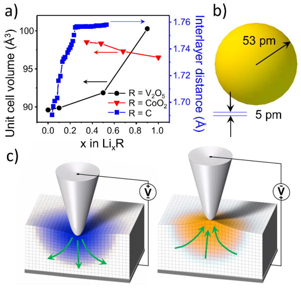
a) Examples of chemical expansion for LixV2O5 (from Ref., ), LixC (graphite, Ref.) and LiCoO2 (Ref.) systems, showing unit cell volume and graphene interlayer distances as a function of Li content; as amount of Li in a material increases, lattice expands or contracts; b) Size comparison of the hydrogen atom (53 pm) and height resolution of modern SPM’s (5 pm); c) ESM detection relies on local volumetric changes in the material due to ion motion in external electric field; a conductive SPM tip in contact with a solid ion conductor can be biased, triggering local repulsion of attraction of ions (green arrows) and causing surface to expand/contract; note that the image exaggerates the extent of volumetric changes. (from Ref. © IOP Publishing. Reproduced with permission. All rights reserved.)

a) a bipolar ESM voltage waveform with a zoomed-in region; the slowly-varying waveform consists of a train of DC steps that excite the system and Band Excitation (BE) AC pulses that probe local lattice expansion; BE pulses are applied when DC voltage is null to avoid electrostatic interactions between the sample and cantilever; b) ESM displacement curves collected on a Si anode in response to the waveform shown in a); progressive loop opening with increasing voltage is due to lithiation/delithiation cycles; c) Map of electrochemical reaction onset voltage in a 500 nm × 500 nm area around a triple boundary junction on a Si anode; d) Single-point curves extracted from the boundary and grain region as indicated in c); Reprinted from Ref.

a) Schematic diagram of tip-induced metal reduction in metal cation (Li+ or Ag+) conductors; Adapted from Ref. © IOP Publishing. Reproduced with permission. All rights reserved; b) Correlation of Li atoms per particle to the number of electrons transferred; The slope (in atoms/electron) is close to 1 in argon atmosphere and is smaller in air. Adapted from Refs., ; c) Topography of the pristine LICGC surface and d) topography recorded after a 100-point IVz spectroscopy measurement. White circles indicate the formed Li particles; e) Current and height change of the sample surface during the application of voltage waveform illustrated in f); Zi, Zmax, and Zf represent the initial height, maximum height, and final height, respectively; c) – f) are adapted with permission from Ref.; Copyright (2013) American Chemical Society
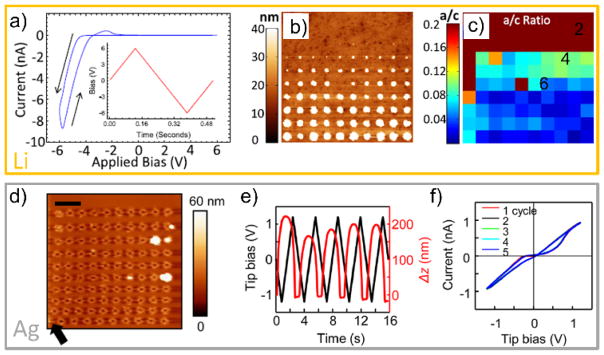
a) I-V curve exhibiting a positive current with an anodic peak upon the return sweep in LICGC. The inset shows the applied triangular bias waveform; b) LICGC topography (16 μm × 16 μm) collected after the 100-point IV spectroscopy measurement. The peak bias is fixed along the fast scan axis (x-axis) but incrementing on the slow scan axis (y-axis); c) Two-dimensional map of the ratio of anodic/cathodic charge transferred for LICGC. a) – c) are adapted from Ref. © IOP Publishing. Reproduced with permission. All rights reserved; d) Ag glass topography (17 μm × 17 μm) recorded after the 100-point IVz spectroscopy measurement. Scale bar is 3.4 μm. Note that the topography at (1,1), indicated by the arrow, was not scanned in the image and the vertical scale is oversaturated to show the crater features; e) The bias waveform used for the measurement of d) and Δz-t curve averaged over the whole 10 × 10 grid; f) The corresponding average I-V curve. d) – f) are adapted with permission from Ref. Copyright (2015) American Chemical Society.
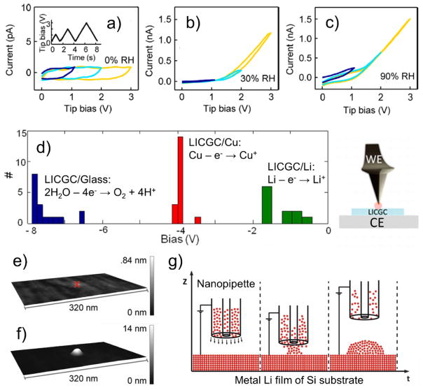
I-V curves averaged over the points of a 10 × 10 grid at different relative humidity: a) 0 %, b) 30 %, and c) 90 %, measured on a AgI-based conducting glass with silver counter electrode; Note the difference in current scales in a) and b), c); The inset in a) shows the FORC-type bias waveform used for the measurements; Sample thickness (separation between the tip and bottom electrode) was ca. 2.5 mm. Adapted with permission from Ref.; Copyright (2015) American Chemical Society; d) Distribution of the nucleation biases for different counter electrodes, Cu, Li, and glass as probed on LICGC in argon atmosphere; Counter-reactions shown; Separation between the tip (working electrode, WE) and counter electrode (CE) was ca. 500 μm; Adapted with permission from Ref. ; Copyright (2013) American Chemical Society; e) and f) Si(111) surface with pre-deposited metal Li film before and after Li particle implantation from the carbon nanotube nanopipette, g) schematics of the process of Li dispensing from the nanopipette; Adapted with permission from Ref. © 2015 WILEY-VCH Verlag GmbH & Co. KGaA, Weinheim.

a) Bias amplitude- and pulse duration-dependent growth of Ag structures induced by single rectangular pulses (inset) in Ag+ glass sample; Detailed description of each growth regime is described provided in Ref. ; b) Topographic image recorded after a negative bias FORC-IVz measurement on a 10 × 10 grid. The chains of unequal silver particles, exhibiting a double periodicity of their lateral sizes, i.e., large-small-large-small, are shown in the dashed open box. Adapted with permission from Ref. ; Copyright (2016) American Chemical Society.
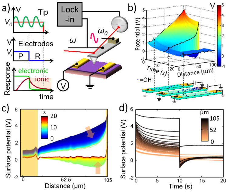
a) A tr-KPFM schematic displaying sample with two lateral electrodes and the AFM cantilever, whose oscillation is coupled to local surface potential and is monitored by a lock-in amplifier; graphs of the voltage excitation signals that are applied to the AFM tip and lateral electrodes are also shown; the response of the electronic and ionic carriers to the excitation will occur on different timescales, allowing their separate detection; b) A 3D response of a Ca-BFO sample to a 5 V excitation that activated electromigration of the surface OH− groups; c) Same response plotted in a 2D graph Potential vs. distance; d) Same response plotted as a 2D graph Potential vs. time for different positions; golden stripes represent lateral electrodes; peach-colored arrows show temporal evolution of the potential profiles; measurements performed at 100 °C. Adapted with permission from Ref. ; Copyright (2013) American Chemical Society.
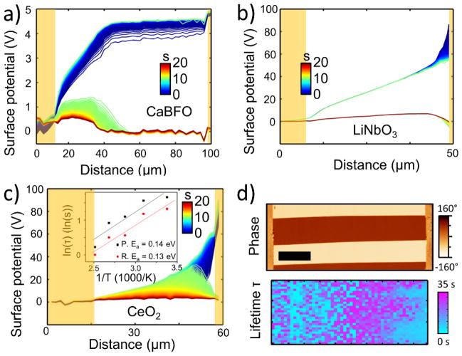
a) Accumulation of (positive) oxygen vacancies in activated Ca-BFO at room temperature; (adapted with permission from Ref. ; Copyright (2013) American Chemical Society) the region of flat blue lines close to the biased electrode is the formed virtual electrode (region of film with metallic conductivity); b) probing injection of protons from the biased electrode in LiNbO3 ferroelectric at room temperature; (adapted with permission from Ref. © 2013 WILEY-VCH Verlag GmbH & Co. KGaA, Weinheim.) c) detection of injection and dissipation of protons in nanostructured ceria at 100 °C; gold stripes represent lateral metal electrodes; the inset shows an Arrhenius plot of the mean lifetime of charged species on Ca-BFO surface with activation energies for the polarization (P.) and relaxation (R.) periods of 0.14 eV and 0.13 eV; d) detection of the difference in screening charge dynamics on a periodically-poled LiNbO3 surface: PFM Phase image correlates with a map of mean lifetime (see right side of the images); (adapted with permission from Ref © 2015 WILEY-VCH Verlag GmbH & Co. KGaA, Weinheim.); ferroelectric domains are seen in the PFM Phase image as brown and beige horizontal bands; metal electrodes are two orange stripes on the left and right borders of the image.
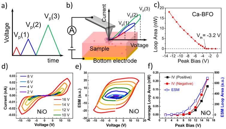
a) An example of a unipolar positive FORC-IV voltage waveform consisting of 3 triangular pulses with increasing peak bias (Vp); b) When a FORC voltage waveform is applied to a conductive AFM tip in contact with the surface of a MIEC, local current can be measured off of the bottom electrode; the FORC-IV curves become hysteretic above the threshold voltage needed for initiation of an electrochemical process; the hysteresis loop area can be used as a measure of local electrochemical activity; c) FORC-IV loop area plotted as a function of the peak bias applied to the tip; the sample is Ca-BFO; d) FORC-IV loops, e) FORC-ESM loops and their dependence on peak bias for a memristive material: NiO thin film; despite the fact that the measured current is electronic, rather than ionic, in this example, the FORC-IV loop area curves correlate well with the ESM hysteresis areas, and are a good measure of local electrochemical activity. Panels a and b are adapted with permission from Ref. ; Copyright (2013) American Chemical Society.

a) Current map at 0.1 V shows higher conductivity on the BFO-CFO tubular interfaces of CFO nanopillars also seen in topographic image e); current maps b)–d) are displayed for the peak biases of 3, 5 and 7 V of the FORC voltage waveform that was used to probe the sample; the FORC-IV loop area maps f)–g) look very different from the current maps and, thus, convey different type of information; map f) is mostly empty, but different interfaces (shown with arrows) start activating at higher voltages – in maps g) and h), manifesting the spatial difference in the onset of the electrochemical process; Note, that neither the current nor the loop area maps contain information on the shape of local IV curves: it was present in the initial dataset, but was lost during data slicing/compression. The 4D FORC-IV datasets (I = f(x, y, V, Vp)) can also be losslessly deconvoluted, into a set of IV curves (endmembers) i)–l) and corresponding loading (intensity) maps using Bayesian Linear Unmixing; These sets of graphs and 2D maps retain all of the information initially present in the FORC-IV dataset; The extracted endmembers can be fitted to appropriate physical models to unravel the local transport behaviors. Panels a) through h) are adapted with permission from Ref. ; Copyright (2013) American Chemical Society. Panels i) through p) are adapted with permission from Ref. ; Copyright (2013) American Chemical Society.

Nanotransport System for in-situ scanning tunneling microscopy and electron spectroscopy of pulsed laser deposition-grown transition metal oxide films.

a) STM topography showing island-type growth mode of the LCMO film grown at pO2 = 50 mTorr; b) High resolution STM image of the same film, showing one disordered termination, and one ordered termination; c) STM topography image of LCMO film grown at lower oxygen partial pressure, with mostly single termination. The atomic scale image of the majority termination is shown in d) indicating a (1 × 1) unreconstructed surface. Scans around edges of islands indicate small patches of second termination e), indicated by the green arrows. These are (√2 × √2) R 45° reconstructions; f) angle-resolved XPS measurements with the O1s peak shown, along with deconvolution into Gaussian-Lorentzian peaks a, b, and c (c only for the 6.7 Pa film); g) Peak area ratios as a function of polar angle. Reprinted (adapted) with permission from Tselev et al.; Copyright (2015) American Chemical Society.
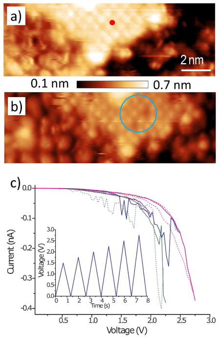
a) An STM image of the (La,Ca)O island is shown in a), and the tip was placed on the red dot indicated before the FORC waveform (inset in c)) was applied. Subsequent STM imaging over the same region, shown in b), revealed the formation of two oxygen vacancies (circled in blue); Reprinted from Vasudevan et al. with the permission of AIP Publishing
Similar articles
-
Toward Electrochemical Studies on the Nanometer and Atomic Scales: Progress, Challenges, and Opportunities.ACS Nano. 2019 Sep 24;13(9):9735-9780. doi: 10.1021/acsnano.9b02687. Epub 2019 Sep 16. ACS Nano. 2019. PMID: 31433942
-
Local electrochemical functionality in energy storage materials and devices by scanning probe microscopies: status and perspectives.Adv Mater. 2010 Sep 15;22(35):E193-209. doi: 10.1002/adma.201001190. Adv Mater. 2010. PMID: 20730814 Review.
-
Emerging Electrochemical Techniques for Probing Site Behavior in Single-Atom Electrocatalysts.Acc Chem Res. 2022 Mar 1;55(5):759-769. doi: 10.1021/acs.accounts.1c00785. Epub 2022 Feb 11. Acc Chem Res. 2022. PMID: 35148075
-
Advanced Electrochemistry of Individual Metal Clusters Electrodeposited Atom by Atom to Nanometer by Nanometer.Acc Chem Res. 2016 Nov 15;49(11):2587-2595. doi: 10.1021/acs.accounts.6b00340. Epub 2016 Oct 27. Acc Chem Res. 2016. PMID: 27786462
-
New electrochemical techniques for probing phase transfer dynamics at dental interfaces in vitro.Adv Dent Res. 1997 Nov;11(4):548-59. doi: 10.1177/08959374970110042401. Adv Dent Res. 1997. PMID: 9470516 Review.
Cited by
-
To switch or not to switch - a machine learning approach for ferroelectricity.Nanoscale Adv. 2020 Apr 15;2(5):2063-2072. doi: 10.1039/c9na00731h. eCollection 2020 May 19. Nanoscale Adv. 2020. PMID: 36132496 Free PMC article.
-
Direct-Write Lithiation of Silicon Using a Focused Ion Beam of Li.ACS Nano. 2019 Jul 23;13(7):8012-8022. doi: 10.1021/acsnano.9b02766. Epub 2019 Jul 10. ACS Nano. 2019. PMID: 31283179 Free PMC article.
-
Nanoscale electrochemical response of lithium-ion cathodes: a combined study using C-AFM and SIMS.Beilstein J Nanotechnol. 2018 Jun 4;9:1623-1628. doi: 10.3762/bjnano.9.154. eCollection 2018. Beilstein J Nanotechnol. 2018. PMID: 29977696 Free PMC article.
-
Nanoscale multistate resistive switching in WO3 through scanning probe induced proton evolution.Nat Commun. 2023 Jul 4;14(1):3950. doi: 10.1038/s41467-023-39687-9. Nat Commun. 2023. PMID: 37402709 Free PMC article.
-
Correlating Nanoscale Structures with Electrochemical Properties of Solid Electrolyte Interphases in Solid-State Battery Electrodes.ACS Appl Mater Interfaces. 2023 Jun 7;15(22):26660-26669. doi: 10.1021/acsami.3c02770. Epub 2023 May 22. ACS Appl Mater Interfaces. 2023. PMID: 37212378 Free PMC article.
References
-
- Zwanenburg FA, Dzurak AS, Morello A, Simmons MY, Hollenberg LC, Klimeck G, Rogge S, Coppersmith SN, Eriksson MA. Rev Mod Phys. 2013;85:961.
-
- O’Brien J, Schofield S, Simmons M, Clark R, Dzurak A, Curson N, Kane B, McAlpine N, Hawley M, Brown G. Phys Rev B. 2001;64:161401.
-
- Fuechsle M, Miwa JA, Mahapatra S, Ryu H, Lee S, Warschkow O, Hollenberg LC, Klimeck G, Simmons MY. Nat Nanotechnol. 2012;7:242–246. - PubMed
-
- Häffner H, Roos CF, Blatt R. Physics reports. 2008;469:155–203.
-
- Chanthbouala A, Garcia V, Cherifi RO, Bouzehouane K, Fusil S, Moya X, Xavier S, Yamada H, Deranlot C, Mathur ND. Nat Mater. 2012;11:860–864. - PubMed
Grants and funding
LinkOut - more resources
Full Text Sources
Other Literature Sources