. 2016 May 6:7:11283.
doi: 10.1038/ncomms11283.

Giant photoluminescence enhancement in tungsten-diselenide-gold plasmonic hybrid structures

Affiliations

Giant photoluminescence enhancement in tungsten-diselenide-gold plasmonic hybrid structures

Zhuo Wang et al. Nat Commun. .

Abstract

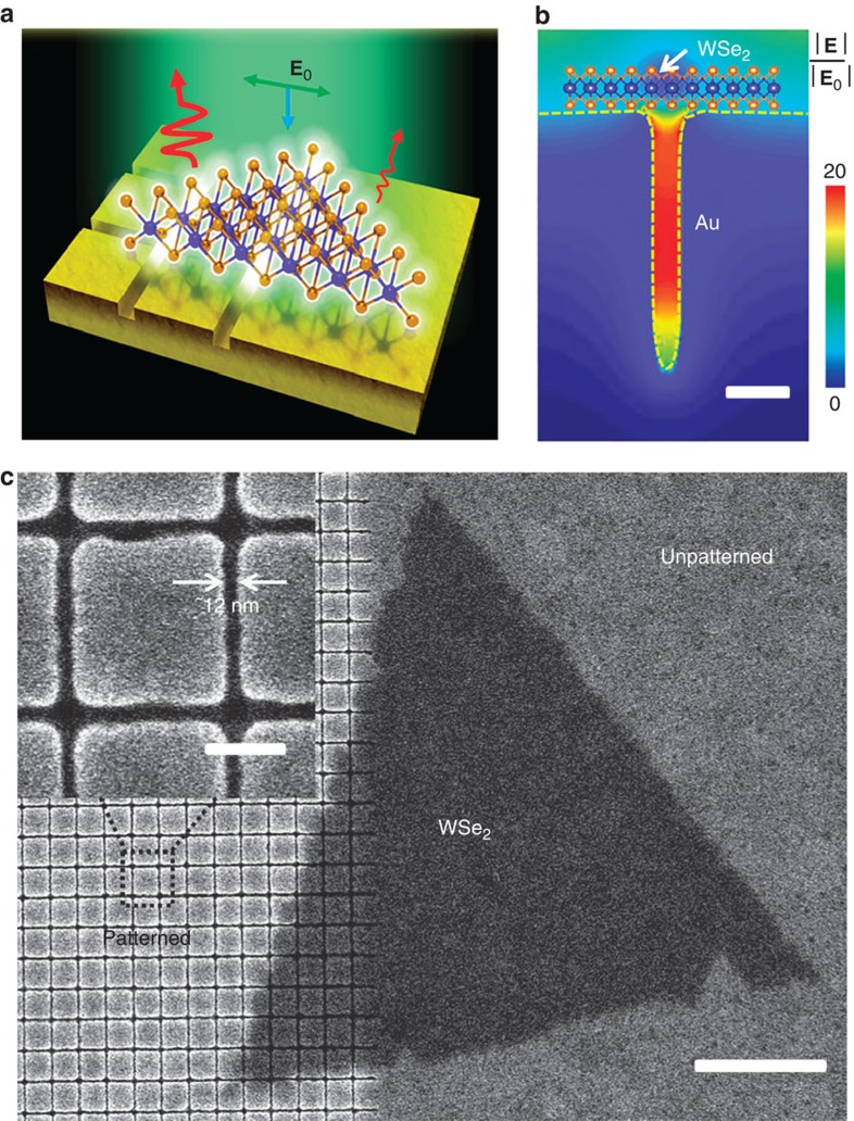
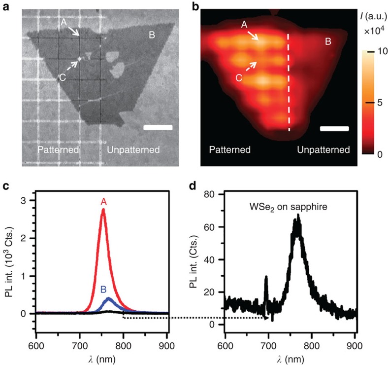
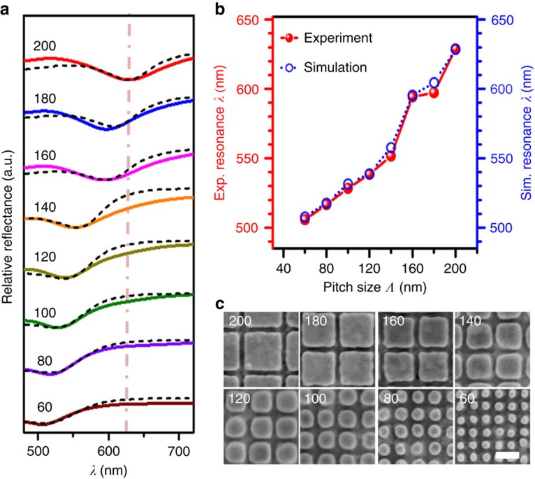
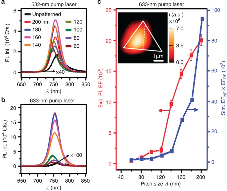
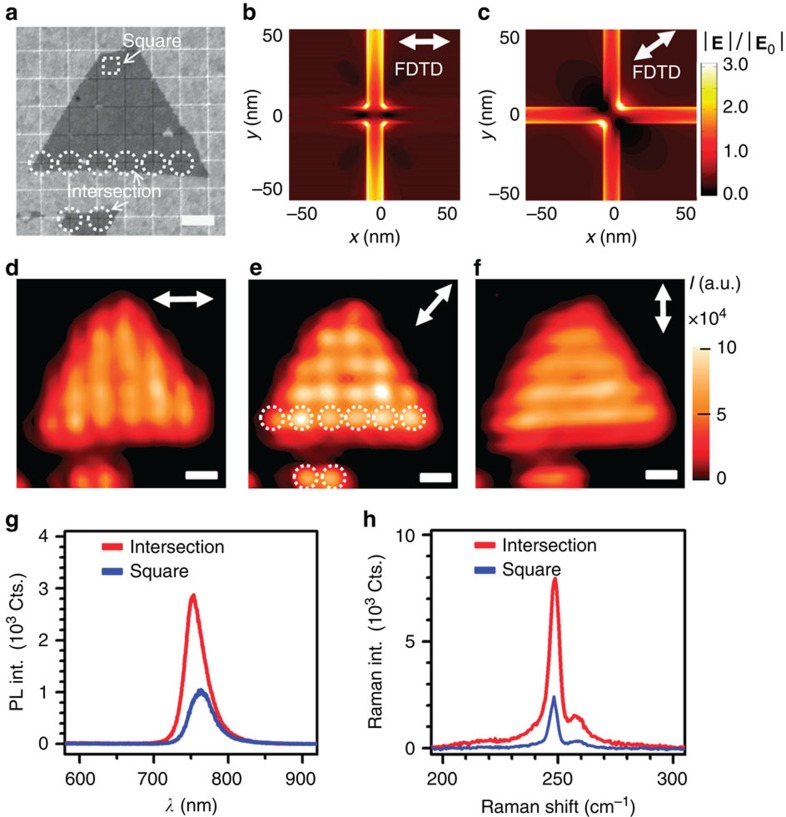
Impressive properties arise from the atomically thin nature of transition metal dichalcogenide two-dimensional materials. However, being atomically thin limits their optical absorption or emission. Hence, enhancing their photoluminescence by plasmonic nanostructures is critical for integrating these materials in optoelectronic and photonic devices. Typical photoluminescence enhancement from transition metal dichalcogenides is 100-fold, with recent enhancement of 1,000-fold achieved by simultaneously enhancing absorption, emission and directionality of the system. By suspending WSe2 flakes onto sub-20-nm-wide trenches in gold substrate, we report a giant photoluminescence enhancement of ∼20,000-fold. It is attributed to an enhanced absorption of the pump laser due to the lateral gap plasmons confined in the trenches and the enhanced Purcell factor by the plasmonic nanostructure. This work demonstrates the feasibility of giant photoluminescence enhancement in WSe2 with judiciously designed plasmonic nanostructures and paves a way towards the implementation of plasmon-enhanced transition metal dichalcogenide photodetectors, sensors and emitters.


Figures

Figure 1
Figure 1. Schematic of WSe2-gold plasmonic hybrid structure with strong optical absorption.
(a) Schematic of PL emission from a single crystal monolayer of WSe2 flake on a gold substrate. Part of the triangular flake rests on the patterned region of the substrate consisting of sub-20-nm-wide trenches. (b) Representative simulation of the electric field distribution of the lateral gap plasmons with a WSe2 monolayer flake suspended over a single trench. The polarization of the incident laser field is across the gap. The dashed yellow line denotes the boundary between air and gold. The scale bar, 20 nm. (c) Representative Scanning electron micrograph (SEM) image of WSe2 on square arrays with a trench width of 12 nm (Patterned) and unpatterned gold film (Unpatterned). The scale bars in the main figure and the inset, 1 μm and 100 nm, respectively.
Figure 2
Figure 2. Characterization results of WSe2-gold plasmonic hybrid structure.
(a) SEM image of a crystalline WSe2 monolayer flake transferred onto a template-stripped substrate with a pitch of 760 nm. ‘A' points to a portion of WSe2 suspended above an intersection of two underlying trenches, while ‘B' corresponds to the reference point, that is, WSe2 on unpatterned smooth gold. ‘C' points to a tear defect in the monolayer. The scale bar, 1 μm. (b) PL intensity (I) mapping on the WSe2-gold plasmonic hybrid structure showing larger signals from patterned regions and resolvable modulations in intensity. The intensity value at each pixel was obtained by integrating the PL spectrum across the spectrum window of 700–820 nm. A 532-nm pump laser was chosen here for a fine PL mapping resolution. (c) PL spectra from WSe2 on patterned gold nanostructures (A), unpatterned gold film (B) and the one from as-grown WSe2 on sapphire. Their PL peak energy (full-width-at-half-maximum) are 1.65 eV (63 meV), 1.63 eV (78 meV) and 1.61 eV (83 meV), respectively. (d) Zoom-in PL spectrum of WSe2 on sapphire. The laser power is 30 μw and integration time is 0.5 s.
Figure 3
Figure 3. Optical characteristics of patterned gold nanostructures with different pitch sizes.
(a) Relative reflectance spectra of patterned gold nanostructures with pitch sizes of 60–200 nm with respect to the unpatterned gold film. The solid and dashed curves present the experimental and simulated spectra, respectively. Legends denote the pitch size in units of nm for each pattern. The dash dot line indicates the position of the pump laser of 633 nm. (b) Experimental (Exp.) and simulated (Sim.) resonance wavelength of the patterned gold nanostructures as a function of pitch size. (c) SEM images of the template-stripped gold nanostructures with respective pitch sizes. The inset numbers denote the pitch sizes in the unit of nm. The scale bar in the SEM images, 100 nm.
Figure 4
Figure 4. Photoluminescence of WSe2 on patterned gold nanostructures with different pitch sizes.
(a) 532-nm pump laser. (b) 633-nm pump laser. (c) Experimental PL enhancement factor (EF) (left axis) excited by 633-nm laser (after correcting for the trench area fraction) and the simulated EFNF (at 633 nm) × EFPF (at 750 nm) (right axis), respectively. The data points and corresponding error bars are obtained, respectively, by calculating the mean value and s.d. of PL EF based on 10 experimental PL spectra for each nanostructure. The inset shows the PL mapping of a WSe2 monolayer flake sited on patterned gold nanostructure with a pitch of 200 nm (on the left of the dashed line) and unpatterned gold film (on the right of the dashed line). The intensity value at each pixel was obtained by integrating the PL spectrum across the spectrum window of 700–820 nm. The solid line represent the shape of the flake and the dashed line represents the boundary between the patterned and unpatterned substrate. The laser power was 30 μW and integration time was 0.5 s.
Figure 5
Figure 5. Polarization-dependent characteristics of PL emission from WSe2 flake on gold nanostructures with a pitch size of 920 nm and a pump laser of 532 nm.
(a) SEM image of WSe2 flake on the gold nanostructures. The white dashed circles denote the region where the trenches in the gold film intersect and the dashed square denotes the centre of the square region. (b,c) Simulated electric field distribution at a plane 1 nm above the surface of patterned gold nanostructures with 0°- and 45°-polarizations, respectively. (df) Corresponding PL intensity mappings with polarization angles of 0°, 45° and 90°, respectively. The intensity value at each pixel was obtained by integrating the PL spectrum across the spectrum window of 700–820 nm. The white arrows show the polarization directions of the pump laser. (g,h) PL and Raman spectra of WSe2 taken at the intersection of gold trenches and square center, respectively. All the scale bars, 1 μm. The laser power and integration time for measuring PL (Raman) is 30 μW and 0.5 s, respectively (450 μW and 15 s).

References

    1. Ross J. S. et al.. Electrically tunable excitonic light-emitting diodes based on monolayer WSe2 pn junctions. Nat. Nanotechnol. 9, 268–272 (2014). - PubMed
    1. Radisavljevic B., Radenovic A., Brivio J., Giacometti V. & Kis A. Single-layer MoS2 transistors. Nat. Nanotechnol. 6, 147–150 (2011). - PubMed
    1. Zhang W. et al.. High gain phototransistors based on a CVD MoS2 monolayer. Adv. Mater. 25, 3456–3461 (2013). - PubMed
    1. Koperski M. et al.. Single photon emitters in exfoliated WSe2 Structures. Nat. Nanotechnol. 10, 503–506 (2015). - PubMed
    1. Chiu M. H. et al.. Determination of band alignment in the single-layer MoS2/WSe2 heterojunction. Nat. Commun. 6, 7666 (2015). - PMC - PubMed

Publication types