. 2016 Apr 15;2(4):e1501882.
doi: 10.1126/sciadv.1501882. eCollection 2016 Apr.

Two-dimensional GaSe/MoSe2 misfit bilayer heterojunctions by van der Waals epitaxy

Affiliations

Two-dimensional GaSe/MoSe2 misfit bilayer heterojunctions by van der Waals epitaxy

Xufan Li et al. Sci Adv. .

Abstract

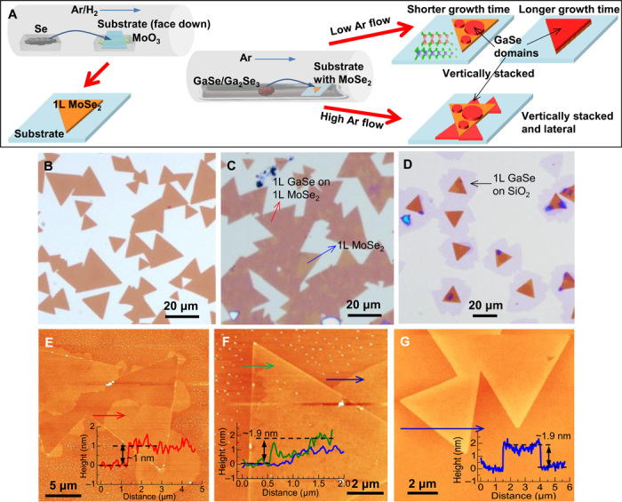
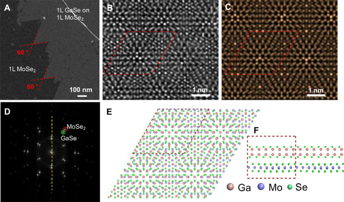
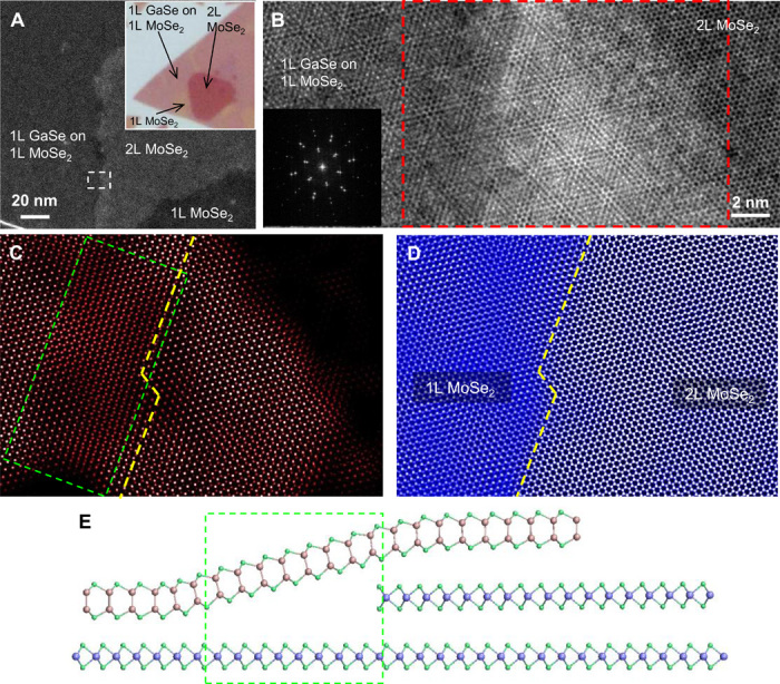
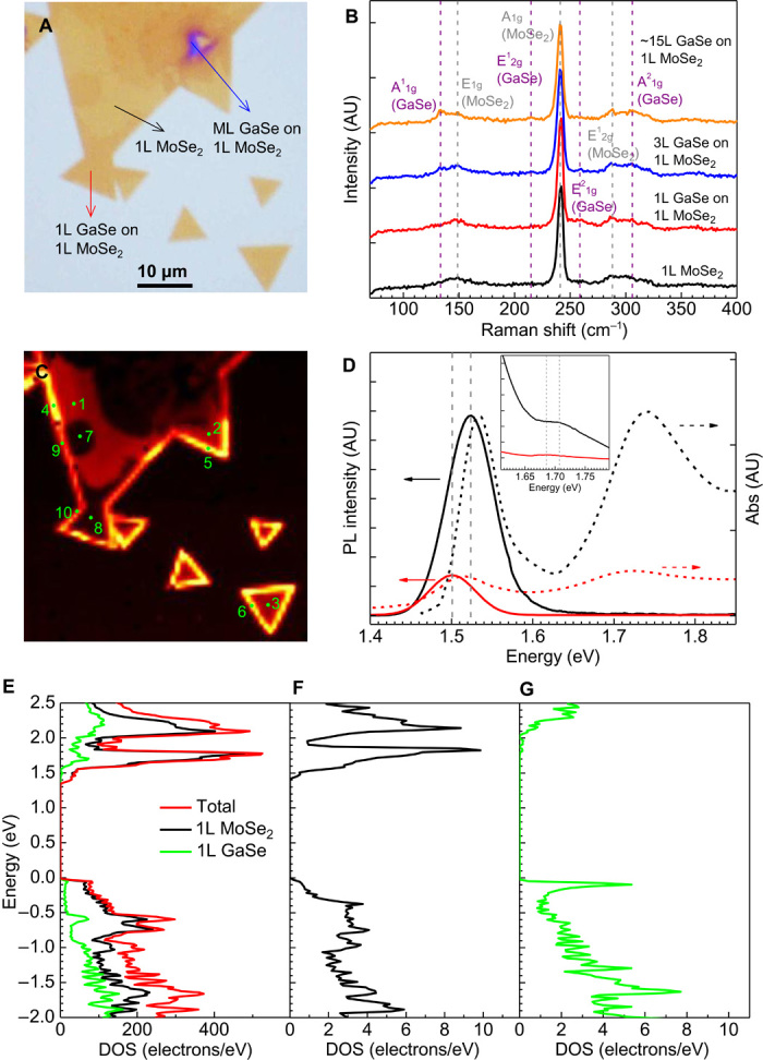
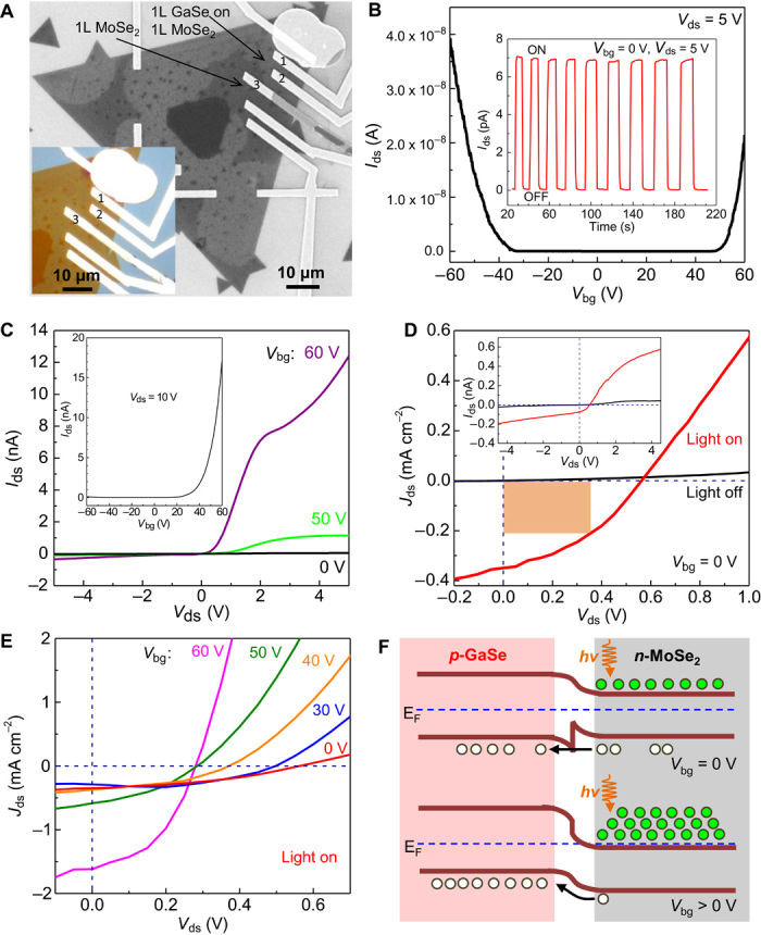
Two-dimensional (2D) heterostructures hold the promise for future atomically thin electronics and optoelectronics because of their diverse functionalities. Although heterostructures consisting of different 2D materials with well-matched lattices and novel physical properties have been successfully fabricated via van der Waals (vdW) epitaxy, constructing heterostructures from layered semiconductors with large lattice misfits remains challenging. We report the growth of 2D GaSe/MoSe2 heterostructures with a large lattice misfit using two-step chemical vapor deposition (CVD). Both vertically stacked and lateral heterostructures are demonstrated. The vertically stacked GaSe/MoSe2 heterostructures exhibit vdW epitaxy with well-aligned lattice orientation between the two layers, forming a periodic superlattice. However, the lateral heterostructures exhibit no lateral epitaxial alignment at the interface between GaSe and MoSe2 crystalline domains. Instead of a direct lateral connection at the boundary region where the same lattice orientation is observed between GaSe and MoSe2 monolayer domains in lateral GaSe/MoSe2 heterostructures, GaSe monolayers are found to overgrow MoSe2 during CVD, forming a stripe of vertically stacked vdW heterostructures at the crystal interface. Such vertically stacked vdW GaSe/MoSe2 heterostructures are shown to form p-n junctions with effective transport and separation of photogenerated charge carriers between layers, resulting in a gate-tunable photovoltaic response. These GaSe/MoSe2 vdW heterostructures should have applications as gate-tunable field-effect transistors, photodetectors, and solar cells.

Keywords: Two-dimensional; heterostructure; lattice-misfit; photovoltaic; van der Waals epitaxy.


Figures

Fig. 1
Fig. 1. Morphology of GaSe/MoSe2 heterostructures.
(A) Schematic illustrating the growth of 1L MoSe2 and GaSe/MoSe2 heterostructures. (B) Optical micrograph of 1L MoSe2 triangular flakes and domains of merged triangles grown on a SiO2/Si substrate. (C) Optical micrograph of 1L GaSe domains (with reddish color contrast as indicated by a red arrow) grown on 1L MoSe2 domains (as indicated by a blue arrow). (D) Optical micrograph of 1L GaSe domains grown on 1L MoSe2 and laterally from the side of 1L MoSe2 on SiO2/Si substrates (as indicated by a black arrow). (E and F) AFM images showing GaSe domains grown on and from the side of 1L MoSe2 flakes. Insets are height profiles along the red, blue, and green lines, indicating that the GaSe domains grown vertically and laterally on MoSe2 are monolayer. (G) AFM image showing 1L GaSe fully covering 1L MoSe2 flakes, as indicated by the height profile along the blue solid line.
Fig. 2
Fig. 2. Atomic structure of the vertically stacked GaSe/MoSe2 vdW heterostructure.
(A) Low-magnification ADF-STEM image showing the edge area of the 1L GaSe domain grown on 1L MoSe2. (B and C) Experimental (B) and simulated (C) atomic-resolution ADF-STEM image showing the atomic structure of the periodic superlattice where 1L GaSe stacks on top of 1L MoSe2. The red dashed rhombuses indicate the unit cell of the GaSe/MoSe2 heterostructure (supercell), with a lattice constant of L = 2.63 nm. (D) FFT pattern obtained from (B). (E and F) Top view and side view of the calculated atomic model of the GaSe/MoSe2 vdW heterostructure, respectively. The supercell is demarcated by the red dashed lines.
Fig. 3
Fig. 3. Atomic structure of the lateral GaSe/MoSe2 heterostructure.
(A) Low-magnification ADF-STEM image showing a 1L GaSe domain connected laterally to a 1L MoSe2 domain where such a heterostructure sits on top of another 1L MoSe2 as an underlying substrate and follows its lattice orientation. Inset: Optical micrograph showing a similar structure in large scale (the red triangle is the 2L MoSe2 region). (B) Atomic-resolution ADF-STEM image of the area highlighted in the white dashed rectangle in (A), showing an overlapping region between the 1L GaSe domain and the bilayer MoSe2 in the lateral connection region (highlighted by the red dashed rectangle). (C and D) Inverse FFT images of 1L GaSe and MoSe2 layers in (B). The green dashed rectangle in (C) highlights the inclined region. The yellow dashed lines in (C) and (D) indicate the position of the step edge in the MoSe2 layers. (E) Schematic of the overlapping structure in the lateral connection region that shows the buckling of 1L GaSe (on 1L MoSe2) stacks on top of the second MoSe2 layer.
Fig. 4
Fig. 4. Optical properties of the GaSe/MoSe2 vdW heterostructure.
(A) Optical micrograph showing 1L MoSe2 islands and flakes with partially covered GaSe domains. The corresponding AFM image shown in fig. S8 was used to measure the number of layers in the GaSe domains. (B) Raman spectra obtained from regions of bare 1L MoSe2 and GaSe domains with different layer numbers on MoSe2 as shown in (A). The excitation source is a 532-nm laser. Note that the spectra were offset for clarity. AU, arbitrary units. (C) PL emission mapping of the area corresponding to (A) with excitation from a 532-nm laser and integrated emission intensity from 700 to 900 nm. (D) PL emission and absorption spectra of bare 1L MoSe2 and 1L GaSe/1L MoSe2 vdW heterostructures. Black solid curve: PL spectrum corresponding to the inner region of bare 1L MoSe2 (spots 1, 2, and 3). Red solid curve: PL spectrum corresponding to the inner region of bare 1L GaSe/1L MoSe2 (spots 7 and 8). The inset shows an enlarged view from 1.6 to 1.8 eV. The PL spectra from the edge area (spots 4, 5, 6, 9, and 10) are shown in fig. S11. Black dashed curve: absorption spectrum of bare 1L MoSe2. Red dashed curve: absorption spectrum of 1L GaSe/1L MoSe2. The absorption spectra were normalized to their A exciton peak. (E) DOS 1L GaSe/1L MoSe2 vdW heterostructure (red solid curve) using DFT calculations. The valence band maximum (VBM) is set at 0 eV. The black and green solid curves are contributions from 1L MoSe2 and 1L GaSe, respectively. (F and G) DOS of independent 1L MoSe2 and 1L GaSe using DFT calculations. The VBM is set at 0 eV.
Fig. 5
Fig. 5. Electrical and optoelectronic properties of the GaSe/MoSe2 vdW heterostructure.
(A) SEM image of a device made on a 1L MoSe2 partially covered by 1L GaSe domains. Electrodes 1 and 2 were made on the GaSe/MoSe2 vdW heterostructure region, whereas electrode 3 was made on a bare 1L MoSe2 region. Inset shows the corresponding optical micrograph. (B) Ids-Vbg curve (with Vds fixed at 5 V) of the vdW heterostructure as a whole measured using electrodes 1 and 2 (without illumination). The inset shows the time-resolved photoresponse of the vdW heterostructure at Vbg = 0 V and Vds = 5 V using a white light source. (C) Ids-Vds curves across the p (GaSe)–n (MoSe2) heterojunction (measured using electrodes 2 and 3) at different back-gate voltages (without illumination). The inset shows the Ids-Vbg curve (with Vds fixed at 10 V) across the heterojunction. (D) Jds-Vds curves (Vbg = 0 V) with (red solid curve) and without (black solid curve) white light illumination across the heterojunction. The area with orange shading indicates Pmax. The inset shows the Ids-Vds curves on a larger scale. (E) Jds-Vds curves with white light illumination across the heterojunction at different back-gate voltages. (F) Equilibrium band diagram of the GaSe/MoSe2 heterojunction at Vbg = 0 V (upper) and Vbg > 0 V (lower) with light illumination.

References

    1. Butler S. Z., Hollen S. M., Cao L., Cui Y., Gupta J. A., Gutiérrez H. R., Heinz T. F., Hong S. S., Huang J., Ismach A. F., Johnston-Halperin E., Kuno M., Plashnitsa V. V., Robinson R. D., Ruoff R. S., Salahuddin S., Shan J., Shi L., Spencer M. G., Terrones M., Windl W., Goldberger J. E., Progress, challenges, and opportunities in two-dimensional materials beyond graphene. ACS Nano 7, 2898–2926 (2013). - PubMed
    1. Radisavljevic B., Radenovic A., Brivio J., Giacometti V., Kis A., Single-layer MoS2 transistors. Nat. Nanotechnol. 6, 147–150 (2011). - PubMed
    1. Hu P., Wang L., Yoon M., Zhang J., Feng W., Wang X., Wen Z., Idrobo J. C., Miyamoto Y., Geohegan D. B., Xiao K., Highly responsive ultrathin GaS nanosheet photodetectors on rigid and flexible substrates. Nano Lett. 13, 1649–1654 (2013). - PubMed
    1. Li X., Lin M.-W., Puretzky A. A., Idrobo J. C., Ma C., Chi M., Yoon M., Rouleau C. M., Kravchenko I. I., Geohegan D. B., Xiao K., Controlled vapor phase growth of single crystalline, two-dimensional GaSe crystals with high photoresponse. Sci. Rep. 4, 5497 (2014). - PMC - PubMed
    1. Morkoç H., Mohammad S. N., High-luminosity blue and blue-green gallium nitride light-emitting diodes. Science 267, 51–55 (1995). - PubMed

Publication types